Optical System Design: Challenges and Advantages

Key Takeaways Optical systems designed with meticulous attention to field of view parameters. Analysis tools utilized to ensure optimal field of view performance. Optimization techniques employed to meet specified field of view requirements effectively. Maximizing Optical System Performance with Zemax At Avantier, we use Zemax for designing, analyzing, and optimizing optical systems, such as lenses, objectives, cameras, and other optical devices.  For optical system design, Zemax helps to construct a virtual optical system by defining optical specifications, such as surface curvatures, thickness, refractive indices, etc. For ray tracing, Zemax simulates the propagation of light rays through the optical system and helps evaluate the imaging performance of the system. For analysis, Zemax offers various analysis tools to evaluate, such as can calculate parameters like wavefront errors, MTF, etc. For optimization, Zemax has the capabilities to improve performance, such as Zemax can automatically adjust the variables (like lens positions, and curvatures) to find the optimal configuration that meets the desired criteria after specifying optimization goals.  For tolerancing, Zemax allows performing tolerance analysis to assess the impact of manufacturing and alignment errors on system performance. Optical System RMS vs Field of view Challenges and Strategies in Optical System Design and Manufacturing Optical technology has become ubiquitous in modern applications, ranging from cameras and telescopes to medical devices and automotive sensors. Nevertheless, crafting these systems poses significant challenges for engineers, notably in rectifying optical flaws and meeting precise specifications. Correcting optical aberrations stands out as a formidable task in the realm of optical engineering. These aberrations, which cause image distortion or blurring, stem from factors like lens curvature, material properties, and refractive indices. Overcoming such imperfections demands a profound grasp of optics, sophisticated mathematical models, and advanced manufacturing methodologies. Addressing optical aberrations involves leveraging both geometrical optics and ray tracing techniques. While geometrical optics simplifies light behavior modeling within optical setups, ray tracing delves deeper, considering material refractive indices. The design journey to rectify optical aberrations entails meticulous steps. Engineers first establish imaging quality requisites, encompassing parameters such as focal length and field of view. They then utilize optical design software to generate initial designs, employing aberration theory to forecast expected flaws. Refinement of these designs hinges on a merit function—a mathematical tool assessing the variance between desired and actual imaging quality. Engineers iteratively adjust parameters until the system meets the predefined specifications. Attaining stringent tolerances represents another formidable aspect of optical engineering. These systems must adhere strictly to accuracy, precision, and repeatability criteria. Achieving such exactness necessitates specialized equipment and expertise across precision engineering, machining, and metrology domains. The optical manufacturing supply chain, intricate and global, spans multiple nations. Raw materials, including glass, plastics, and metals, are sourced globally. Manufacturing entails diverse processes like lens grinding, polishing, and surface coating with anti-reflective materials, culminating in optical system assembly. Future Trends and Innovations in Optical System Design and Manufacturing In conclusion, designing and manufacturing optical systems is a complex and challenging process. Correcting optical aberrations and achieving tight tolerances require a deep understanding of optics, advanced mathematical models, and sophisticated manufacturing techniques. As demand for optical systems continues to grow on a large scale, the supply chain and manufacturing industry will continue to evolve and improve to meet the demands of the market. RELATED CONTENT:

Read more
How to Read an Optical Drawing

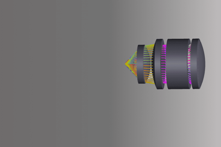
An optical drawing is a detailed plan that allows us to manufacture optical components according to a design and given specifications. When optical designers and engineers come up with a design, they condense it in an optical drawing that can be understood by manufacturers anywhere.  ISO 10110 is the most popular standard for optical drawing. It describes all optical parts in terms of tolerance and geometric dimension. The image below shows the standard format of an optical drawing. Notice thee main fields. The upper third, shown here in blue, is called the drawing field. Under this the green area is known as the table field, and below this the title field or, alternately, the title block (shown here in yellow). Once an optical drawing is completed, it will look something like this: Notice the three fields— the drawing field, the table field, and the title field. We’ll look at each of them in turn. Field I — Drawing Field The drawing field contains a sketch or schematic of the optical component or assembly. In the drawing here, we see key information on surface texture, lens thickness, and lens diameter. P3 means level 3 polished, and describes the surface texture. Surface texture tells us how close to a perfectly flat ideal plane our surface is, and how extensive are the deviations. 63 refers to the lens diameter, the physical measurement of the diameter of the front-most part of the lens 12 refers to the lens thickness, the distance along the optical axis between the two surfaces of the lens After reviewing the drawing field we know this is a polished bi-convex lens, and we know exactly how large and how thick it is. But there is more we need to know before we begin production. To find this additional information, we look at the table field. Field 2— Table Field In our example, the optical component has two optical surfaces, and table field is broken into three subfields. The left subfield refers to the specifications of the left surface, and the right subfield refers to the specifications of the right surface. The middle field refers to the specifications of the material. Surface Specifications: Sometimes designers will indicate “CC” or “CX” after radius of curvature, CC means concave, CX means convex. Material Specifications: 1/ : Bubbles and Inclusions Usually written as 1/AxB where A is the number of allowed bubbles or inclusions in lens B is the length of side of a square in units of mm 2/ : Homogeneity and Striae Usually written as 2/A;B where A is the class number for homogeneity B is the class for striae Field 3: Title Field The last field on an optical drawing is called the title field, and it is here that all the bookkeeping happens. The author of the drawing, the date it was drawn, and the project title will be listed here, along with applicable standards. Often there will also be room for an approval, for a revision count, and for the project company. A final crucial piece of information is the scale: is the drawing done in 1:1, or some other scale? Now you know how to read an optical drawing and where to find the information you’re looking for. If you have any other questions, feel free to contact us!

Read more
Case Study: Objective Lens Design
Optical Design, Custom optical design solutions, Optical Engineering, Custom Optical Lens Design

Design for Manufacturing (DFM) Case Study: Objective Lens Design for Trapping and Imaging Single Atoms At Avantier we offer Design for Manufacturing (DFM services), optimizing product design with our extensive knowledge of manufacturing constraints, costs, and methods. Avantier Inc. received a request from a University Physics department to custom design a long working distance, high numerical aperture objective. Our highly skilled and knowledgeable engineers designed and deployed state-of-the-art technologies to develop a single-atom trapping and imaging system where multiple laser beams are collimated at various angles and overlapped on the dichroic mirrors before entering the objective lens. The objective lens focuses the input laser beams to create optical tweezers arrays to simultaneously trap single atoms and image the trapped atoms over the full field of view of the microscope objective. The objective lens not only had high transmission but also can render the same point-spread function or diffractive-limited performance for all traps over the full field of view.  Typical requirements for the objective lens used for trapping and imaging single atoms:  Custom objective lens example Objective lens focuses high-power laser beams to create optical tweezers at 6 wavelengths (i.e., 420nm, 795nm, 813nm, 840nm, 1013nm, and 1064nm) and image the trapped atoms at the wavelength of 780nm. 

Read more
Lossless Image Compression Example

For storage and transmission of large image files it is desirable to reduce the file size. For consumer-grade images this is achieved by lossy image compression when image details not very noticeable to humans are discarded. However, for scientific images discarding any image details may not be acceptable. Still, all the images, except completely random ones, do include some redundancy. This permits lossless compression which does decrease image file size while preserving all the image details. The simplest file compression can be achieved by using well-known arithmetic encoding of the image data. Arithmetic encoding compression degree can be calculated using Shannon entropy, which is just minus averaged base 2 Log of probabilities of all the values taken by the image pixels. This Shannon entropy gives averaged number of bits per pixel which is necessary to arithmetically encode the image. If, say, the original image is a monochrome one with 8 bits per pixels, then for completely random image the entropy will be equal to 8. For non-random images the entropy will be less than 8. Let’s consider simple example of NASA infrared image of the Earth, shown here using false color This image is 8-bit monochrome one, and has entropy of 5.85. This means arithmetic encoding can decrease image file size 1.367 times. This is better than nothing but not great. Significant improvement can be achieved by transforming the image. If we would use standard Lossless Wavelet compression (LWT), after one step of the LWT the initial image will be transformed into 4 smaller ones: 3 of these 4 smaller images contain only low pixel values which are not visible on the picture above. Zooming on them saturates top left corner, but makes small details near other corners visible (notice the changed scale on the right): Now the entropy of the top left corner 5.85, which is close to the entropy 5.87 of the complete initial image. The entropies of the other 3 corners are 1.83, 1.82 and 2.82. So, after only one LWT step the lossless compression ratio would be 2.6, which is significantly better than 1.367. Our proprietary adaptive prediction lossless compression algorithm shows small prediction residue for the complete image: Actual lossless compression ratio achieved here is about 4.06. It is remarkable that while the last picture looks quite different from the original NASA image, it does contain all the information necessary to completely recover the initial image. Due to lossless nature of the compression, the last picture, using arithmetic encoding, can be saved to the file 4.06 times smaller than the initial NASA picture file. Our proprietary algorithm applied to this smaller file completely recovers the initial picture, accurately to the last bit. No bit left behind.

Read more
Case Study: Infrared Lens Design

  Design for Manufacturing (DFM) Case Study: Infrared Lens Design for Scientific Equipment At Avantier we offer Design for Manufacturing (DFM services), optimizing product design with our extensive knowledge of manufacturing constraints, costs, and methods. Measuring the relative concentrations of carbon monoxide, products of combustion and unburned hydrocarbons is the basis of flare monitoring and is typically accomplished with infrared spectral imaging. For real time continuous monitoring, a multispectral infrared imager can be used.  We were approached by a scientific equipment supplier for DFM help on a particular infrared lens (50 mm f/1) that is used in their infrared imager. The lens was designed to offer the high image quality and low distortion needed for scientific research, but though it performed as desired, there were two major manufacturing problems that made it expensive to produce. The first issue was expensive aspheric lens elements. The second was the inclusion of GaAs to improve the modulation transfer function (MTF) and to correct chromatic aberration. GaAs is a highly toxic material, and incorporating it in the design complicates the manufacturing process and increases the cost.  Taking into account both lens performance and our client’s manufacturing budget, Avantier redesigned the infrared lens with DFM principles. Our final design included no aspheric lens elements and no hazardous material, but we met all requirements for distortion, MTF, and image height offset at the working spectral lens. Using a combination of 5 spherical lens elements and 1 filter, our 50 mm f/1 lens was able to reduce the lens cost by about 60%. In the below image the configuration of the 50 mm f/1 lens is shown. For a wavelength range of approximately 3 to 5 µm the MTF was 0.7, well within our client’s requirements. The next image below shows the modulation transfer function (MTF) plots for the redesigned lens. This last image below shows the lens distortion plot. The maximum field was 6.700 degrees, and the maximum f-tan distortion 0.6526%. Whatever your need might be, our engineers are ready to put their design for manufacturing experience to work for you. Call us to schedule a free initial consultation or discuss manufacturing possibilities. 

Read more