Silicon Carbide Wafers
Silicon carbide (SiC) wafers are a specialized semiconductor material known for their high thermal conductivity, and superior power and frequency performance. These wafers are essential in electronic devices requiring high-temperature and high-voltage operations. SiC’s wide bandgap makes it a superior choice for handling higher voltages and extreme conditions compared to traditional materials like silicon.
Orientation of SiC substrate | |
Crystal Orientation | Orientation crystallography of the SiC substrate the Angle of inclination between the c axis and the vector perpendicular to the wafer surface (see Figure 1). |
Orthogonal Orientation Deviation | When the crystal face intentionally deviates from the (0001) crystal face, the Angle between the normal vector of the crystal face projected on the (0001) plane and the direction [11-20] nearest to the (0001) plane. |
Off-Axis | < 11-20 > Direction deviation 4.0°±0.5° |
Positive Axis | <0001> Direction off 0°±0.5° |
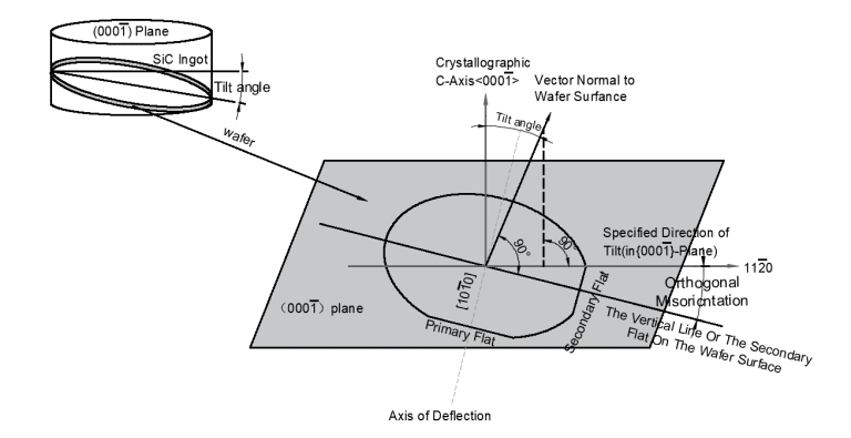
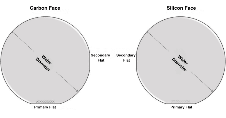
Diameter | Measure the wafer diameter with a standard vernier caliper (see Figure 2). |
Primary Flat | The edge has the longest length on a wafer whose crystal surface is parallel to the {1010} lattice plane. |
Orientation of Primary Flat | The orientation of Primary Flat is always parallel to the < 1120 > direction (or parallel to the {1010} lattice plane). Primary Flat was measured by XRD back reflection technique |
Secondary Flat | Its length is shorter than that of the main positioning edge, and its position relative to the Primary Flat can distinguish the Si and C surfaces (Figure 2). |
Orientation ofSecondary Flat | With Si face up, the orientation of the Secondary Flat can be rotated 90° clockwise along the Primary Flat. |
Marking | For Si surface polishing materials, the C surface of each wafer is marked with laser marking (Figure 2). |
Production Methods: PVT and CVD
The production of SiC wafers involves advanced techniques such as physical vapor transport (PVT) and chemical vapor deposition (CVD). In the PVT method, a seed crystal of SiC is placed in a high-temperature furnace, and vaporized silicon and carbon are transported by a carrier gas, typically argon, to form a SiC layer. In the CVD method, silicon and carbon gases react on a substrate at high temperatures, resulting in the growth of a high-quality SiC layer. These methods are designed to minimize defect density, ensuring the production of high-quality wafers.
Wafer Processing and Fabrication
After the SiC crystals are grown, they are sliced into thin wafers and polished to achieve a high degree of flatness and smoothness. These SiC wafers serve as a robust platform for further semiconductor layering, which is crucial for power devices that require high thermal conductivity and efficient operation. The wafers can be doped to create P-type and N-type regions, essential for fabricating high-performance electronic devices.
Advantages and Limitations of SiC Compared to Silicon
Silicon carbide (SiC) wafers offer several advantages over silicon, particularly in high-temperature, high-voltage, and high-frequency applications. SiC’s superior thermal conductivity allows it to perform efficiently without the risk of thermal breakdown, making it ideal for power devices in electric vehicles and other high-power applications. Despite these benefits, silicon remains the more commonly used semiconductor material in lower temperature environments due to its simpler preparation process. However, as the demand for energy-efficient solutions in renewable energy and other sectors grows, SiC is becoming increasingly important in the semiconductor industry.
Factory Standards
P-type 4H-SiC, Single Crystal |
P-type 6H-SiC, Single Crystal |
N-type 3C-SiC, Single Crystal |
|
Lattice Parameters |
a=3.082 Å c=10.092 Å |
a=3.09 Å c=15.084 Å |
a=4.349 Å |
Stacking Sequence |
ABCB |
ACBABC |
ABC |
Mohs Hardness |
≈9.2 |
≈9.2 |
≈9.2 |
Density (g/cm3 ) |
3.23 |
3.0 |
3.17 |
Therm. Expansion Coefficient |
4.3×10⁻⁶/K(⊥C axis)4.7×10⁻⁶/K(∥C axis) |
4.3×10⁻⁶/K(⊥C axis)4.7×10⁻⁶/K(∥C axis) |
3.8×10⁻⁶/K |
Refraction Index@750nm |
no = 2.621, ne = 2.671 |
no=2.612,ne=2.651 |
n=2.615 |
Dielectric Constant |
c~9.66 |
c~9.66 |
c~9.66 |
Thermal Conductivity(W/cm·K@298K ) |
3-5 |
3-5 |
3-5 |
Band-Gap (eV) |
3.26 |
3.02 |
2.36 |
Break-Down Electrical Field (V/cm) |
2-5×10⁶ |
2-5×10⁶ |
2-5×10⁶ |
Saturation Drift Velocity (m/s) |
2.0×10⁵ |
2.0×10⁵ |
2.7×10⁷ |
SiC Wafers Specifications
Dummy Grade (D Grade) | 6-inch Diameter | 4-inch Diameter | 2-inch Diameter | |
|---|---|---|---|---|
Diameter | 145.5 mm ~ 150.0 mm | 93.5 mm ~ 100.0 mm | 50.8mm ±0.38mm | |
Thickness | 350 µm ± 25 µm | 350 µm ± 25 µm | 350 µm ± 25 µm | |
Wafer Orientation | Off axis: 2.0 ~ 4.0° toward (1102) ± 0.5° for 4H/6H(P, N) On axis (111) ± 0.5° for 3C-N | Off axis: 2.0 ~ 4.0° toward (1102) ± 0.5° for 4H/6H(P, N) On axis (111) ± 0.5° for 3C-N | Off axis: 2.0 ~ 4.0° toward (1102) ± 0.5° for 4H/6H(P, N) On axis (111) ± 0.5° for 3C-N | |
Micropipe Density※ | 0 cm-² | 0 cm-² | 0 cm-² | |
Resistivity※ | p-type 4H/6H-P | ≤0.3 Ω·cm | ≤0.3 Ω·cm | ≤0.1 Ω·cm |
n-type 3C-N | ≤1 Ω·cm | ≤1 Ω·cm | ≤0.8 Ω·cm | |
Primary Flat Orientation | 4H/6H-P | {1010} ± 5.0° | {1010}± 5.0° | {10-10} ± 5.0° |
3C-N | {110} ± 5.0° | {110} ± 5.0° | {1-10} ± 5.0° | |
Primary Flat Length | 32.5 mm ± 2.0 mm | 32.5 mm ± 2.0 mm | 15.9 mm ± 1.7 mm | |
Secondary Flat Length | 18.0 mm ± 2.0 mm | 18.0 mm ± 2.0 mm | 18.0 mm ± 1.7 mm | |
Secondary Flat Orientation | Silicon face up: 90° C.W. from Prime Flat ± 5.0° | Silicon face up: 90° C.W. from Prime Flat ± 5.0° | Silicon face up: 90° C.W. from Prime Flat ± 5.0° | |
Edge Exclusion | 6 mm | 6 mm | 5 mm | |
LTV/TTV/Bow/Warp | ≤10 µm/≤15 µm/≤25 µm/≤40 µm | ≤10 µm/≤15 µm/≤25 µm/≤40 µm | ≤2.5 µm/≤5 µm/≤5 µm/≤30 µm | |
Roughness | Polish | Ra≤1 nm | Ra≤1 nm | Ra≤1 nm |
Roughness | CMP | Ra≤0.5 nm | Ra≤0.5 nm | Ra≤0.5 nm |
Edge Cracks By High Intensity Light | Cumulative lengths ≤ 10 mm, single length≤2 mm | Cumulative lengths ≤ 10 mm, single length≤2 mm | 1 allowed, ≤1 mm | |
Hex Plates By High Intensity Light※ | Cumulative area ≤ 0.1% | Cumulative area ≤ 0.1% | Cumulative area ≤ 3% | |
Polytype Areas By High Intensity Light※ | Cumulative area ≤ 3% | Cumulative area ≤ 3% | Cumulative area ≤ 5% | |
Visual Carbon Inclusions | Cumulative area ≤ 3% | Cumulative area ≤ 3% | Cumulative area ≤ 3% | |
Silicon Surface Scratches By High Intensity Light※ | Cumulative length ≤ Wafer diameter | Cumulative length ≤ Wafer diameter | 8 scratches ≤ 1 Wafer diameter cumulative length | |
Edge Chips By High Intensity Light | 5 allowed, ≤1 mm each | 5 allowed, ≤1 mm each | 5 allowed, ≤1 mm each | |
Silicon Surface Contamination By High Intensity | None | None | None | |
Packaging | Multi-wafer Cassette or Single Wafer Container | Multi-wafer Cassette or Single Wafer Container | Multi-wafer Cassette or Single Wafer Container |
Customizing SiC Wafers
Avantier is one of the leading companies in SiC wafer production, offering customization to meet your specific requirements. Whether you need specialized wafers for high-power, high-frequency, or high-temperature applications, our expertise ensures high-quality results. Contact us for your next project, and let us help you achieve optimal performance with our SiC wafers.
WE CAN HELP YOU!
Contact us NOW for sales & expert advice.


