Customized rod lenses in endoscopy facilitate light transmission for precise visualization of internal structures.
Key Takeaways: Avantier specializes in premium medical optics, collaborating with clients for tailored solutions. Optics are pivotal in modern medicine, driving diagnostic breakthroughs and treatment advancements. High-quality optics are essential for applications like endoscopy, OCT, PCR, robotic surgery, and ophthalmology. Manufacturing precision is crucial, balancing quality, cost, and timeline under stringent regulatory standards. Avantier exemplifies cost-efficient production, swift customization, adherence to performance standards, and regulatory compliance. Introduction Avantier, a distinguished manufacturer of high-precision medical optics, collaborates with clients to produce cutting-edge optical components and devices tailored to their precise specifications. This scientific reading material explores the pivotal role of optics in modern medicine, delves into the intricate process of manufacturing optics, presents exemplary applications, and emphasizes the critical factors of cost, timeline, performance, and regulatory standards. Medical Optics in Modern Medicine Optics plays a paramount role in contemporary medical advancements, serving as the cornerstone of diagnostic breakthroughs. Medical optics, comprising a range of optical technologies, finds extensive utilization in medical research, diagnostics, and treatment. Avantier proudly manufactures top-tier optical components for medical devices and offers custom solutions to cater to diverse medical needs. Applications of High-Quality Medical Optics High-performance optics underpin medical advancements across various domains, including research, diagnostics, and treatment. Medical professionals benefit from advanced techniques facilitated by robust optical components. These optics feature prominently in applications such as micro endoscopy, optical coherence tomography (OCT), polymerase chain reaction (PCR) instruments, robotic surgery, and laser-based ophthalmology. Manufacturing Precision Medical Optics Manufacturing optics for medical devices demands an unwavering commitment to quality. The precision of optical components is of utmost importance, as human lives rely on their flawless operation within diagnostic and treatment protocols. Stringent standards govern the production of medical optics, balancing the imperative of superior quality with budget and time constraints. Effective medical optics design harmonizes these factors to deliver high-performance optics at a competitive price with rapid turnaround. Exemplary Medical Optics Applications Avantier exemplifies the creation of medical optics meeting the highest standards within budget and time constraints. A notable application is optical coherence tomography, a noninvasive diagnostic technique offering cross-sectional retinal imaging. This aids in the diagnosis and treatment of conditions like macular degeneration and diabetic eye disease. Furthermore, laser-assisted eye surgery, supported by advanced medical optics, has supplanted traditional cataract surgery. Optical coherence tomography assists in mapping the eye’s structures before precise laser interventions for improved patient outcomes. Cost Considerations The sensitivity to cost within medical services necessitates an approach that optimizes benefit-cost ratios. Avantier ensures cost-efficient production of medical device optics through comprehensive design and engineering expertise. Timeline and Performance The development of medical devices and research endeavors operates under strict time constraints. Avantier offers a broad range of readily available optical components for medical devices and specializes in swift customization. Our design and engineering team collaborates with clients to expedite product development plans while maintaining exceptional performance standards. High-performance optics and lens assemblies for medical use are indispensable for reliable laboratory and clinical applications, preventing equipment failures that could obscure research findings or lead to catastrophic clinical outcomes. Quality Standards Medical optics adhere to stringent regulatory standards to ensure device reliability. Avantier holds ISO 13485 certification, signifying our ability to consistently produce high-quality optics in medical use compliant with customer requirements and regulatory mandates. State-of-the-art metrology equipment guarantees that our medical optical components conform to all relevant standards, facilitating their seamless integration into medical research, diagnostic, and treatment applications. Custom validation processes are available to further ensure quality and compliance. In conclusion, the collaboration between Avantier underscores the pivotal role of precision medical optical components in advancing the field of medicine. The commitment to quality, cost efficiency, timeline adherence, and regulatory compliance positions these manufacturers at the forefront of medical optics innovation, ultimately benefiting both patients and the scientific community. Related Content: Optical Coherence Tomography (OCT) Flow Cytometry Part1: Illuminating Cellular Diversity and Analysis Fluorescence Microscopy Part 1: Illuminating Samples for High-Resolution Imaging
The optimization of parabolic mirror telescopes ensures exceptional image quality for astronomical observation.
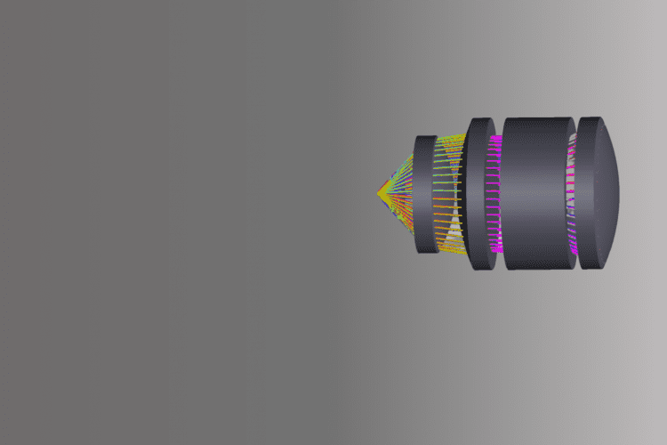
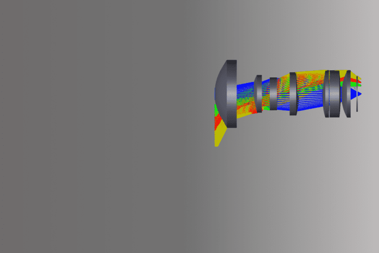
Blurring is a significant source of image degradation in an imperfect imaging system. The optical system’s point spread function (PSF) describes the measure of blur in a given imaging system and is often used in image reconstruction or image recovery algorithms. Below in example of using inverse PSF to eliminate the barcode image degradation. Barcodes are found on many everyday consumer products. A typical 1-D (one-dimensional) barcode is a series of varying width vertical lines (called bars) and spaces. The example of the popular GS1-128 Symbology barcode is shown here: The signal amplitude of code image only has changes in horizontal direction (i.e. X-direction). For the imaging system used to capture and decode the barcode it is sufficient to look at one-dimensional intensity profile along the X-direction. In good conditions the profile may look like this: Using such a good scan, it is trivial to recover initial binary (only Black and only White) barcode. One can set threshold in the middle between maxima and minima of the received signal, and assign whatever is above the threshold to White, and below the threshold to Black. However, in situations when the Point Spread Function (PSF) of the imaging system is poor, it may be difficult or impossible to set the proper threshold. See example below: PSF is the impulse response of an imaging system, it contains information of the image formation, systematic aberrations and imperfections. To correctly decode barcode in such situations one may try to use inverse PSF information to improve the received signal. The idea is to deduce inverse PSF from the multiple signals obtained from the many scans of different barcodes of the same symbology. All barcodes of the same Symbology, such as GS1-128, have the same common features defined by the Symbology standards. This permits us to calculate inverse PSF coefficients by minimizing deviation of the received signals from the ideal barcode profile signals. A small number, such as 15, of the inverse PSF coefficients may be used to correct the received signals to make them as close to barcode signals as possible in the Least Squares sense. The inverse PSF coefficients were found and used to convert poor received signal shown previously into better signal shown on the next picture by red: While the recovered red signal is not ideal, it does permit to set threshold and correctly recover the scanned barcode.
An optical drawing is a detailed plan that allows us to manufacture optical components according to a design and given specifications. When optical designers and engineers come up with a design, they condense it in an optical drawing that can be understood by manufacturers anywhere. ISO 10110 is the most popular standard for optical drawing. It describes all optical parts in terms of tolerance and geometric dimension. The image below shows the standard format of an optical drawing. Notice thee main fields. The upper third, shown here in blue, is called the drawing field. Under this the green area is known as the table field, and below this the title field or, alternately, the title block (shown here in yellow). Once an optical drawing is completed, it will look something like this: Notice the three fields— the drawing field, the table field, and the title field. We’ll look at each of them in turn. Field I — Drawing Field The drawing field contains a sketch or schematic of the optical component or assembly. In the drawing here, we see key information on surface texture, lens thickness, and lens diameter. P3 means level 3 polished, and describes the surface texture. Surface texture tells us how close to a perfectly flat ideal plane our surface is, and how extensive are the deviations. 63 refers to the lens diameter, the physical measurement of the diameter of the front-most part of the lens 12 refers to the lens thickness, the distance along the optical axis between the two surfaces of the lens After reviewing the drawing field we know this is a polished bi-convex lens, and we know exactly how large and how thick it is. But there is more we need to know before we begin production. To find this additional information, we look at the table field. Field 2— Table Field In our example, the optical component has two optical surfaces, and table field is broken into three subfields. The left subfield refers to the specifications of the left surface, and the right subfield refers to the specifications of the right surface. The middle field refers to the specifications of the material. Surface Specifications: Sometimes designers will indicate “CC” or “CX” after radius of curvature, CC means concave, CX means convex. Material Specifications: 1/ : Bubbles and Inclusions Usually written as 1/AxB where A is the number of allowed bubbles or inclusions in lens B is the length of side of a square in units of mm 2/ : Homogeneity and Striae Usually written as 2/A;B where A is the class number for homogeneity B is the class for striae Field 3: Title Field The last field on an optical drawing is called the title field, and it is here that all the bookkeeping happens. The author of the drawing, the date it was drawn, and the project title will be listed here, along with applicable standards. Often there will also be room for an approval, for a revision count, and for the project company. A final crucial piece of information is the scale: is the drawing done in 1:1, or some other scale? Now you know how to read an optical drawing and where to find the information you’re looking for. If you have any other questions, feel free to contact us!
An IR lens is an optical lens designed to collimate, focus, or collect infrared light. At Avantier Inc., we produce high performance IR Optics such as IR lenses for use with near-infrared (NIR), short-wave infrared (SWIR), mid-wave infrared (MIR), and long-wave infrared (LWIR) spectra. These Infrared lenses can be customized for specific areas of the infrared spectrum, and are suitable for applications in defense, life science, medical, research, security, surveillance and other industries. Why Choose Avantier for Your Infrared Optics Needs Whether you require one-off production of single infrared (IR) lens assembly for a specialized research project or a large quantity of fixed-focus IR lenses for industry use, you need to know you can count on your provider. When you work with Avantier, you know you are getting the best product possible, at the best possible price. Our engineers design for manufacturability and work hard to ensure you get an optimized product at an optimal price and within an optimal time frame. That’s because we’ve done it, again and again. Our extensive experience in infrared optics enables us to both design and produce the highest quality lenses and assemblies for IR light. State of the art metrology and a robust quality control program means that every lens with the Avantier name on it will perform exactly as intended, and we check and double check that each component meets your full specification. Our manufacturing processes meet all applicable ISO and MIL standards, and our IR lenses are well known throughout the world. Types of Infrared Lenses Infrared light is classified as light between the wavelengths of 1 mm to about 700 nm. Infrared IR radiation can be further divided into several categories: The substrate chosen for a lens will depend partly on which IR region it is designed for. For instance, Calcium Fluoride (CaF2) lenses are a good choice for radiation between 80 nm – 8 μm and so would be ideal for NIR SWIR wavelengths. Zinc Selenide has optimal transmission from 8 – 12μm, although it offers partial transmission over 0.45 μm to 21.5 μm and Zinc Sulfide (good transmission in 8-12µm, or partial transmission from 0.35 to 14µm). Avantier and IR Lens Design Our experienced engineers and consultants can help you determine the best substrate and antireflective or reflective coating best fits your application. Every situation is unique, and we can help you find a cost effective solution that meets your need. Whether you need special resistance to mechanical and thermal shock, or good performance in rugged environments, we can select the perfect substrate for you. We can also help design your IR lens or optical lens assembly. From basic lens selection (singlet, aspherical lens, spheric lens, cylindrical lens, custom shape lens) to design of aspheric lenses arranged in a complex opto-mechanical device, or any other infrared optical assembly, we have you covered. Avantier can provide lenses in chalcogenide material. Chalcogenide is an amorphous glass and is easier to process than traditional IR crystalline materials. Chalcogenide glass is an ideal material for both high performance infrared imaging systems and high volume commercial applications. Chalcogenide glass is available in a variety of chemical composition options, but BD6, composed of arsenic and selenium (As 40 Se 60), is the best choice in terms of cost and ease of production. Chalcogenide infrared glass materials and lenses are also an excellent alternative to expensive, commodity price-driven materials such as Ge, ZnSe, and ZnS2. Chalcogenide glass primarily transmits in the MWIR and LWIR wavelength bands, making it suitable for infrared imaging applications. Please contact us if you’d like to schedule a free consultation or request for a quote on your next project.
Identifying Resolution of Imaging Systems Resolution is a measurement of an imaging system’s ability to resolve the object which is be imaged. Test targets are typically tools that are used to check the resolution of an imaging system. The most popular targets consist of “groups” of 6 “elements” and each element consists of three horizontal and three vertical bars equally spaced with well-defined width. The vertical bars are used to calculate horizontal resolution and horizontal bars are used to calculate vertical resolution. Analyzing test target image is to identify the Group Element number of highest spatial frequency where either horizontal or vertical lines are distinguishable. Here is an example of such test target image: To look at the pixel values we have chosen one row which is close to the center of the image. We see that the maximum pixel brightness is 120 counts at the center and about 95 counts at the edge for the test target image. Maximum theoretical pixel value for an 8-bit format image is 255 counts, thus only half of the sensor dynamic range is used for this test. Groups are labeled by numbers in order of increasing frequency. It is obvious that Groups with highest resolution are near the image center. The image part, where the groups 8 and 9 are located, is shown here: To avoid repetitions, we only show the calculation results for the resolution along the horizontal / X direction. To reduce the noise in calculation of the image contrast, each group image of the 3 vertical bars was averaged along Y direction inside the extent of the black bars. The resulting averaged amplitudes along X direction for all the elements of the group 8 are shown here: The signal amplitude difference between black stripe/line and white space is recognizable for the 6 elements of Group 8, i.e., all the 6 elements are distinguishable Next picture shows the same kind of plot for all the elements of the group 9: The signal amplitude difference between black bar/line and white space is countable for the elements 1-5 but is not distinguishable for the element 6 of group 9. The resolution of this imaging system is Group-9 Element-5 with line width of 0.62µm, i.e., frequency of 806 line pairs per mm. It is known that the resolution of an imaging system can be affected by factors such as object/test target contrast, lighting source intensity, and software correction. Increasing the illumination intensity and having proper parameter settings for the camera can improve the resolution of the imaging system.
Design for Manufacturing (DFM) Case Study: Objective Lens Design for Trapping and Imaging Single Atoms At Avantier we offer Design for Manufacturing (DFM services), optimizing product design with our extensive knowledge of manufacturing constraints, costs, and methods. Avantier Inc. received a request from a University Physics department to custom design a long working distance, high numerical aperture objective. Our highly skilled and knowledgeable engineers designed and deployed state-of-the-art technologies to develop a single-atom trapping and imaging system where multiple laser beams are collimated at various angles and overlapped on the dichroic mirrors before entering the objective lens. The objective lens focuses the input laser beams to create optical tweezers arrays to simultaneously trap single atoms and image the trapped atoms over the full field of view of the microscope objective. The objective lens not only had high transmission but also can render the same point-spread function or diffractive-limited performance for all traps over the full field of view. Typical requirements for the objective lens used for trapping and imaging single atoms: Custom objective lens example Objective lens focuses high-power laser beams to create optical tweezers at 6 wavelengths (i.e., 420nm, 795nm, 813nm, 840nm, 1013nm, and 1064nm) and image the trapped atoms at the wavelength of 780nm.
Today’s advanced driver assistance systems take advantage of AI-spiked cameras and radar or sonar systems, but most manufacturers have been waiting for advances in machine vision technology to go one step further into autonomous self-driving cars. Today, that technology is ready to roll out. We call it LiDAR: Light detection and ranging. LIDAR in autonomous vehicles can create a 3D understanding of the environment of the LiDAR systems, providing a self-driving car with a dynamic, highly accurate map of anything within 400 meters. Understanding LiDAR LiDAR works by sending out laser pulses that reach a target, then bounce back to where a LiDAR sensor measures the time it took for the round trip. This enables the LiDAR system to create a point map that gives the exact location of everything within the reach of the laser beam. While the reach depends on the laser type used, those used in autonomous cars can now provide accurate data on objects up to 400 meters distance. Since LiDAR systems use laser light from a moving source on the car to ‘see’, the technology is not dependent on ambient light and can function just as well at night as during the day. LiDAR is used in more than just self-driving cars. It has become important in land surveying, forestry and farming, and mining applications. LiDAR technology was used to discover the topology of Mars, and is being used today in a program studying the distances between the surfaces of the moon and earth. It can provide soil profiling, forest canopy measurements, and even cloud profiling. LiDAR in Autonomous Vehicles Ten years ago, LiDAR was expensive and clunky, but that didn’t stop autonomous driving pioneers from incorporating it into their prototypes. Google designed a car with a $70,000 LiDAR system sitting right on top of the vehicle, and ran a series of very successful tests in Mountain View, California and around the U.S. There was just one problem: tacking an extra $70,000 bill onto an already expensive car leads to something that is simply not practical for anything besides research. Today, Waymo manufactures self-driving cars using what they learned from those original experiments, and each of these cars is fitted with a similar LiDAR system. The design has been improved over the years, but the most glaring change is a very promising one: advances in technology have enabled Waymo to bring the cost of the LiDAR system down 90%. Now LiDAR technology is available to any manufacturer of LiDAR cars, and our LiDAR optical design specialists can help you come up with a LiDAR system that meets your budget and requirements. Contact us for more information or to chat with one of our engineers.
How Peak to Valley (PV) and Root Mean Square (RMS) Affect the Quality of Your Optics Just how smooth is the surface of your optic? Qualitative descriptions are of limited value, and often you’ll want to put a number to it. Two ways of quantifying deviations from an ideal optical surface are peak-to-valley (PV) and root-mean-square (RMS). While root-mean-square provides more information, peak-to-valley measurements have been used more often historically. Both methods have their pros and cons. Here we’ll look into both in more detail. Understanding Peak to Valley (PV) Measurements A peak to valley measurement represents the distance between the highest point and lowest point on the surface of an optic. Theoretically, this number should be quite useful: for instance, it allows an optical designer to make worse case predictions on optical performance. In practice, though, it is much more problematic. Using peak to valley measurements assumes that all measurements are precise and the surface has no noise. It is most useful if there are large sized features on the optics, or if the order of aberration is low. An actual optic will have numerous imperfections that are closer than a millimeter to the aperture. Measurements from peak to value will be taken with an instrument that is far from ideal; typically, it will have a significant noise level and a large MTF difference. Because of the inherent problems with measurement, optical manufacturers typically have their own measuring method which does little but mask the condition of the optic. Often the measuring instruments are only used to interpolate the standard parameters in a method based more on a study of optical properties rather than the actual optic under consideration. Unfortunately cost and manufacturability are often expected to depend entirely on the value of PV. For instance, we have had customers come in with a minimum budget requesting a 1/10 wave PV optic, with no specifications on testing conditions. This type of demand can only lead to a prohibitively expensive optic, an unworkable project, or the specification reinterpreted by the vendor. Standard manufacturing processes do not admit for 1/10 wave PV. Understanding Root Mean Square (RMS) Measurements A root mean square (RMS) measurement describes the average deviation of the actual optical surface from an ideal surface. While PV gave the ‘worst case scenario’, we can think of RMS as providing the overall surface variation. RMS values are also dependent on measurement, and especially on the relative area of the optic sampled. However, they are typically much more informative than PV values. While some may attempt to convert between PV and RMS measurements by multiplying by 3.5, this is inaccurate and misleading. The two numbers are measuring very different things, and there is a simple relationship between them. A surface may have a large gouge that results in a large PV, but if the rest of the optic is smooth the RMS will reflect that. Similarly, if a surface has a relatively small PV but the surface is completely rough, the RMS will be larger than expected by a look at the PV. Comparing RMS and PV Measurements Below are images which show the plot of 1 micron PV for basic terms of aberration, as well as the corresponding RMS. We see RMS is noticeably different for each basic term of aberrations. When computer-controlled sub-aperture polishing comes into play, we often see cyclic errors. The below plots again show 1-micron PV, but here we have different frequencies of cyclic error. Though you can align pretty much all of the basic aberration in your optical system, cyclic form error will typically not be compensated for. In these images you can see that the PV and RMS measurements end up being essentially the same as basic aberration terms. Now consider the below image, which shows the stimulated plot of an optic where the error consists of many small imperfections and a few larger, localized imperfections. A well fabricated optic will typically be of this kind. In this situation, the PV is still close to the 1 micron we saw in our other plots; RMS, however, is much less. These plots demonstrate how RMS reflects the actual surface quality of the optical system, while PV provides hardly any useful information. RMS is a better specification than PV, but as always, the key is to partner with a trustworthy optics supplier that can work with you to manufacture an optic with the best performance possible at your price point. At Avantier Inc., that’s what we do every day. Contact us for a free consultation, and put our 50+ years of optical experience to work for you.