Throughput Decoupling: Multi-Mirror Array High-NA Objectives for Sub-3nm Metrology
Key Takeaways
Throughput Decoupling:Next-generation High-NA Multi-Mirror Array Objectives break the resolution-speed trade-off, reducing 12-inch wafer inspection to <8 minutes.
Yield Economics: High-NA optics increase defect capture from 70% to 99.2%, driving 15–20% annual yield recovery in sub-3nm nodes.
Broad-Spectrum 3D Metrology: Aplanatic correction across 200–1100nm enables non-destructive characterization of Chiplets and high-aspect-ratio trenches.
Adaptive Precision: Future objectives integrate MEMS-based actuators to counteract thermal drift, achieving sub-0.3nm CD measurement stability.
1. The Stochastic Barrier: Resolution vs. Throughput
In the <3nm regime, the primary bottleneck in defect metrology is no longer just the diffraction limit, but the signal-to-noise ratio (SNR) at high scan speeds. Traditional single-channel inspection forces a compromise between sensitivity and TACT (Total Actual Cycle Time).
The industry shift toward Multi-Mirror Array (MMA) Coordination and multi-beam scanning architectures has fundamentally decoupled the FOV from the resolution.
Throughput Benchmarks: By implementing multi-path interference and high-speed CMOS integration, 12-inch wafer inspection cycles have been reduced from 30 minutes to <8 minutes.
Yield Correlation: This high-speed high-fidelity capture increases the lithographic defect detection rate from 70% to 99.2%, translating to an estimated 15%-20% annualized yield recovery for leading-edge nodes.
2. Chromatic and Geometric Aberration in Wide-Spectrum 3D Metrology
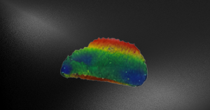
The rise of Heterogeneous Integration (Chiplets/TSV) requires inspection optics to maintain diffraction-limited performance across a broad spectral band (200nm – 1100nm) to facilitate deep-trench penetration and non-destructive 3D characterization.
Aplanatic Correction: Achieving total aberration correction across this band while maintaining NA ≥ 1.35 requires advanced apochromatic designs using low-dispersion fluorite elements.
CD Metrology Precision: In integrated SEM-optical systems, objective lens stability has enabled a reduction in Critical Dimension (CD) measurement error from 5nm to < 0.3nm, pushing the boundaries of ISO 19749:2021 compliance.
3. Opto-Mechanical Constraints: The “Glass Ceiling”
For Mechanical Engineers, the challenge lies in the thermal and structural stability of the lens housing during high-acceleration stages.
Material Bottlenecks: The performance gap between international Tier-1 objectives and emerging alternatives is currently quantified by a 0.2 nm resolution delta and a 0.1-0.15 NA deficit, largely due to the availability of ultra-high refractive index (HRI) glass and aspherical polishing tolerances.
Adaptive Compensation: Future-state objectives are pivoting toward intelligent adaptive correction, utilizing internal MEMS actuators to compensate for thermal drift and focus-shift in real-time during 24/7 fab operations.
4. Technical Roadmap: Projecting the Next Gradient
The evolution of objective make-up is tracking toward four critical KPIs required for the 2nm and 1nm (Angstrom) eras:
Metric
Current State-of-the-Art
Target Specification (Next Gen)
Numerical Aperture (NA)
≥ 1.45
≥ 1.55
Working Distance (WD)
≥ 5mm
10mm – 20mm
Spectral Range
DUV to NIR (200nm – 1100nm)
Full Spectrum / Adaptive
Resolution (Electronic)
≤ 0.1nm
≤ 0.01nm
Conclusion
The trajectory of semiconductor metrology is no longer defined solely by the physics of the diffraction limit, but by the engineering synergy of optical precision, mechanical stability, and high-speed data throughput. As the industry transitions toward 2nm architectures and complex 3D integration, the objective lens must evolve from a passive imaging component into an intelligent, adaptive subsystem. Successfully navigating the trade-offs between ultra-high Numerical Aperture and long working distances remains the critical frontier in maintaining sustainable yields for the next generation of global fab production.
Technical Inquiry
We are currently benchmarking our next-generation objective specifications against emerging sub-3nm requirements. To discuss specific opto-mechanical constraints or to review our latest MTF (Modulation Transfer Function) data under fab-simulated thermal conditions, please contact our engineering team for a technical consultation.