
Used in various applications, including computer-controlled systems, traffic lights, and scenarios requiring manipulation of light beams.

Used in various applications, including computer-controlled systems, traffic lights, and scenarios requiring manipulation of light beams.
Field Dynamics of F-theta Scanning Lens. Join us to explore the field dynamics of F-theta scanning lenses for a wider perspective.
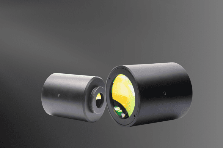
Explore laser technology with the F-theta scanning lens: precision design, wavelengths, and applications for optimal performance.

Explore compact, high-definition Small Microscope Objective Lenses in medical optics, redefining precision in diagnostics and treatments.

The Small Objective Lens, a key component of optical microscopes, facilitates microscopic exploration of the microcosm.

Aspheric lenses( aspherical lenses) reduce spherical aberration in optical systems, providing an alternative to traditional objective lenses.

Telescopes utilize optics, including mirrors, and undergo customization for optimized performance based on specific needs.
Resolution and contrast are crucial considerations in optical system design, evaluated using the Modulation Transfer Function (MTF).
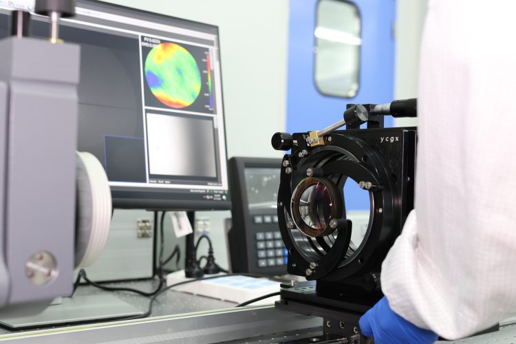
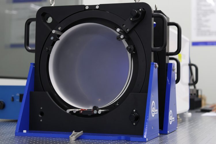
Optical metrology equipment facilitates non-contact, precise measurements crucial for ensuring quality and accuracy in various applications.
Optical science encompasses geometric optics, physical optics, and quantum optics, each with distinct focuses and applications.
