Key Takeaways
- Precision Performance: Achieves diffraction-limited imaging using High-NA Cryogenic Quantum Optics to maximize photon collection efficiency.
- Environmental Stability: FEA-optimized housings ensure sub-nanometer wavefront stability from room temperature down to 4K.
- Broadband Correction: Tailored multi-wavelength optimization (UV-NIR) supports simultaneous cooling, trapping, and state readout.
- Scalable Integration: Engineered for seamless implementation in trapped-ion, neutral atom, and solid-state quantum platforms.
Optimizing High NA, Long Working Distance, and Environmental Stability
1. Introduction: The Optical “Trilemma” in Quantum Systems
In quantum computing architectures—specifically trapped-ion, neutral atom, and solid-state systems—the optical interface is the primary determinant of system fidelity. The engineering challenge is rarely about a single parameter; it is about resolving the “trilemma” between High Numerical Aperture (NA), Long Working Distance (WD), and Extreme Environmental Constraints. This article outlines the design methodology required to achieve diffraction-limited performance without compromising the physical requirements of quantum hardware.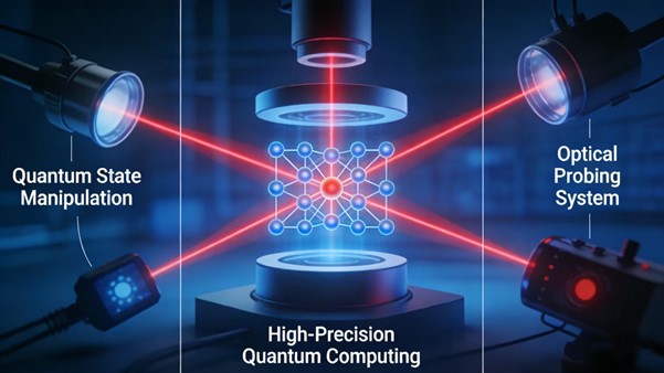
2. Core Engineering Challenges & Solutions
2.1 Bridging the Gap: High NA vs. Long Working Distance
For high-fidelity state readout, an NA > 0.7 is often required to maximize photon collection. However, physical interference with vacuum windows, cryogenic shields, or magnetic coils necessitates a WD of 10mm or more.- Design Strategy: By utilizing Aspheric Elements and Diffractive Optical Elements (DOE), we correct high-order spherical aberrations that occur when expanding the effective focal length. This allows us to push the WD to several times the length of standard microscope objectives while maintaining near-theoretical NA limits.
2.2 Stability Under Cryogenic and UHV Conditions
Quantum processors operate in extreme environments, from Ultra-High Vacuum (10⁻¹² mbar) to Cryogenic temperatures (4K). Standard optics fail here due to outgassing and thermal-induced stress.- Material Science & FEA: We utilize low-thermal-expansion alloys and specialty polymers for lens housings. Every design undergoes Finite Element Analysis (FEA) to predict and compensate for wavefront distortion (λ/4 RMS) and focal shift caused by thermal contraction from 300K down to 4K.
2.3 Multi-Wavelength Management for Discrete Transitions
A single objective lens must often handle a spectrum ranging from Deep UV (369nm for Yb+) to NIR (1064nm for optical traps). Conventional achromatic designs are insufficient for the discrete, high-precision needs of quantum gates.- Achromatic Optimization: Our designs are optimized for specific atomic transition lines (e.g., 369nm, 422nm, 780nm) simultaneously. This ensures that cooling, pumping, and detection lasers stay co-axial and co-focal, eliminating the need for mechanical realignment during experiments.
3. Platform-Specific Implementation
Platform | Primary Optical Constraint | Custom Solution |
Trapped-Ion | Limited spatial access within UHV chambers. | Integrated vacuum-sealed objective units with high collection efficiency. |
Neutral Atom | Uniformity over large 2D/3D qubit arrays. | Large Field-of-View (FoV) designs with minimal distortion for DMD/AOD addressing. |
Solid-State | Compatibility with MW/RF control fields. | Non-magnetic housing and multi-physics optimized optical paths. |
4. Metrology and Validation
To guarantee performance, we employ high-resolution Wavefront Sensing and interferometric testing.- Sensitivity: Sub-nanometer wavefront diagnosis.
- Stability: Real-time holographic measurement to verify beam quality under simulated thermal drift, ensuring long-term entanglement stability.
5. Conclusion: From Proof-of-Concept to Scalable Engineering
The transition of quantum technology from the lab to commercial scalability depends on robust optical engineering. By balancing interdependent metrics—NA, WD, and environmental resilience—we provide the foundational hardware necessary for high-fidelity quantum measurement and control.
Ready to Optimize Your Quantum Architecture?
Don’t let optical constraints limit your qubit fidelity. Whether you are scaling trapped-ion chains or engineering 3D neutral atom arrays, our engineers are ready to collaborate on your next-generation system. [Contact our engineering team to discuss your custom specifications]


