
Understanding focal length: zoom lenses offer variable focal lengths, while fixed focal lengths and shorter focal lengths affect the FOV.

Avantier Inc.
Understanding focal length: zoom lenses offer variable focal lengths, while fixed focal lengths and shorter focal lengths affect the FOV.

Avantier showcases innovative efficiency in custom high NA long working distance objective lens development for microscope manufacturers.

Used in various applications, including computer-controlled systems, traffic lights, and scenarios requiring manipulation of light beams.

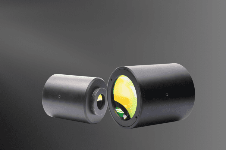
Avantier’s high-quality fisheye lens effectively addresses chromatic aberration and distortion, ensuring superior image quality.

Discover the innovative F-theta lens design with a forward compensating element for expanded field of view in this article
Field Dynamics of F-theta Scanning Lens. Join us to explore the field dynamics of F-theta scanning lenses for a wider perspective.
Explore laser technology with the F-theta scanning lens: precision design, wavelengths, and applications for optimal performance.

Explore compact, high-definition Small Microscope Objective Lenses in medical optics, redefining precision in diagnostics and treatments.
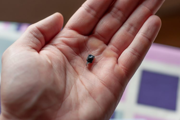
The Small Objective Lens, a key component of optical microscopes, facilitates microscopic exploration of the microcosm.

Aspheric lenses( aspherical lenses) reduce spherical aberration in optical systems, providing an alternative to traditional objective lenses.