High Resolution Microscope Objective Manufacturing

Key Takeaways Avantier specializes in high-precision microscope objectives. Our process involves detailed optical and mechanical design, precise lens fabrication, meticulous structural part machining, careful lens group assembly and debugging, rigorous installation and adjustment, and final re-inspection and secure packaging. Our state of the art design and manufacturing processes ensure high-performance objectives for diverse applications. Introduction to Manufacturing High Resolution Microscope Objectives With over two decades of experience in optical engineering and manufacturing, our company specializes in the design and production of high-precision microscope objectives. Our portfolio encompasses a wide range of standard and specialized objectives, from conventional 2X to 100X flat field designs to advanced supercomplex metachromatic objectives. This article provides a detailed technical overview of our manufacturing process, focusing on the production of a 20X microscope objective as a representative example.  Optical Design The process of designing a new objective begins with meticulous optical design, driven by customer specifications and application requirements. Requirement Analysis: Optical engineers analyze customer-defined parameters, including usage requirements, lens specifications, and acceptance criteria. Design and Simulation: Utilizing advanced optical design software (e.g., ZEMAX), engineers develop and optimize the optical system. Tolerance Analysis: Critical to manufacturability, engineers refine tolerances for optical components, ensuring ideal performance within production capabilities.Engineering Drawings: Aided by state of the art design software,  the team generates detailed engineering drawings for all optical elements. ZEMAX Screenshot of 20X Optical Design   Architectural Design Even as the optical design process is underway, structural engineers develop the mechanical design of the objective. Mechanical Requirements: Structural design factors in all customer-specified mechanical parameters, including external dimensions and interface threads. Manufacturing Constraints: Engineers optimize structural tolerances, surface treatments, and material selection based on production processes. Engineering Drawings: Comprehensive engineering drawings for all structural components are created. CAD Screenshot of 20X Objective Structural Design Lens Processing When the design of the objective is complete, it is time for fabrication to begin. The fabrication of high-quality lenses is a multi-stage process requiring precision and control. Process Planning: Process engineers generate detailed process diagrams, including lens drawings, tooling requirements, and manufacturing sequences. Material Preparation: Raw optical materials are cut to precise dimensions according to process drawings. Grinding: Coarse Grinding: Initial shaping of the lens blank is done using coarse grinding methods. Fine Grinding: Precise shaping of the lens radius (R value) and thickness is accomplished by fine grinding that may be computer-guided. Lens Grinding Polishing: After the lens is shaped, the required surface finish is achieved through various polishing techniques (classical, low throw, high throw). Lens Polishing Edging: The outer diameter of the newly polished lens is then ground to specified dimensions. Lens Edging Inspection: After the edging is finished, rigorous testing using interferometers, projectors, micrometers, and calipers is done to verify lens dimensions and surface quality. Lens Outer Diameter Test Cleaning: Ultrasonic cleaning is used to remove contaminants, and this cleaning is followed by cleanliness inspection. Coating: For many lenses, the next step in the process is the application of optical coatings using vacuum deposition techniques to meet spectral requirements. Coating Test Cementing: Bonding multiple lens elements is accomplished using UV-curable adhesives, with precise centering adjustments. Blackening: Application of black ink to lens edges is done to minimize stray light. Lens Edge Blackening Final Inspection and Storage: When the edging is complete, we run a comprehensive inspection of lens parameters and surface cleanliness, followed by packaging and storage in a controlled environment. Lens Surface Wipe Inspection Structural Parts Processing Producing a microscope objective also involves the fabrication of mechanical components, which  is performed using precision machining techniques. Process Planning: Process engineers develop detailed process drawings and tooling requirements. Material Preparation: Raw materials are cut to specified dimensions. Machining: Precision machining is done with lathes, milling machines, and other equipment. Metal Working Workshop Inspection: All parts are subject to dimensional and geometric verification using coordinate measuring machines (CMMs) and other metrology equipment. Surface Treatment: After inspection, surface treatments such as anodizing, sandblasting, and electroplating are done as required. Final Inspection and Storage: Comprehensive inspection and packaging is done in a controlled environment. Mirror Group Assembly and Debugging: The assembly of lens elements into optical groups is a critical step. Assembly Techniques: Two important techniques are employed in assembly: point glue repair and optical axis turning. Point Glue Repair: Point glue repair involves precision alignment and bonding using UV-curable adhesives. Semi-Automatic Glue Repair Machine Optical Axis Turning: Precision machining is done to ensure concentricity and perpendicularity of lens elements. Lens Installation and Adjustment: Objective Debugging: Assembly and adjustment of the objective lens is accomplished using a microscope frame and star target observation. Objective Point Adjustment Perfect Star-Dot Image Image with Coma Aberration Resolution Testing: A resolution target is used to evaluate and test the objective resolution. Resolution Target Image Under 20X Objective Focal Length Adjustment: The objective lens focal length is adjusted through precision machining. Re-inspection and Packaging: Before an objective lens leaves our factory, final quality control and packaging ensure product integrity. Re-inspection: Comprehensive testing of assembled objectives is done using star target observation and MTF testing. Objective Lens MTF Detection Packaging: The objective is securely packed to ensure comprehensive protection during shipping and storage. 20X Objective Packaging Carton 20X Objective Packaging Bottles Manufacturing High Resolution Microscope Objectives The manufacturing of high precision microscope objectives is a complex and demanding process requiring expertise in optical design, precision machining, and assembly. Our company’s commitment to quality and continuous improvement ensures the delivery of high-performance objectives for a wide range of applications. Related Content

Read more
 Space Tech Expo USA 2025

Join Avantier at the Space Tech Expo USA for an exciting exhibition! Date: June 3 – 4, 2025 | Booth: No. 758Location: Long Beach Convention Centre, California We are excited to welcome you to our booth, where you can explore our innovative optical solutions. Don’t miss out on exclusive giveaways!  Our team is looking forward to discussing the latest advancements in our products and services, and how they can enhance your projects and help you achieve your goals. To discuss your upcoming projects with us, please schedule an appointment using the form below or click here. For further trade show details, please click here (the Space Tech Expo USA website). Loading… Featured Products

Read more
LiDAR Sensor for Robotics

KeyTakeaways LiDAR for Robotics: LiDAR (Light Detection and Ranging) enables precise mapping by using laser light, offering reliable vision even in darkness or challenging environments.   1D LiDAR: Measures distance using a single laser pulse, ideal for collision avoidance, UAV altitude measurement, and industrial inspection.   2D LiDAR: Scans a plane by rotating, improving spatial awareness for security, motion detection, and autonomous vehicles.   3D LiDAR: Creates full 3D maps, simplifying setup and replacing multiple sensors.   Advanced LiDAR: Includes Flash, OPA, and MEMs LiDAR for enhanced imaging. A LiDAR sensor for robotics is more than simply another mechanical imaging system. LiDAR, short for Light Detection and Ranging, uses light in much the same way radar uses radio waves— to create a highly accurate, highly reliable map of surrounding objects. Since it relies on its own laser light source rather than ambient light, it can “see” even in darkness and when the atmosphere is opaque to visible light. Less prone to interference than ultrasonics, it is well suited to robotic vision, especially where precision and reliability are at a premium.  Advances in robotics promise more effective systems with the potential for more autonomy, and it is in these effective, semi-autonomous systems that require minimal guidance that foul-proof vision systems are becoming of more and more importance. Developments in LiDAR sensors have made this technology, once inaccessible except to the best funded research, well within the reach of any industrial or research application. In this article we’ll look at several different types of LiDAR sensors— 1D, 2D, and 3D sensors— and how they function in various robotic applications.  LiDAR sensors for robotics can be used to provide reliable information on the environment in which a robot is used 1D LiDAR Sensors A one-dimensional LiDAR is a compact economical system with one basic function— to measure the distance between it and an object directly in front of it by line of sight. It accomplishes this by sending one-directional pulses of laser light and detecting the time of flight when the pulse is reflected back. This can be converted to an incredibly precise, real time distance measurement.  One dimensional LiDAR systems can be used for dependable collision avoidance as well as for altitude measurement on UAVs, basic surveillance, industrial or agricultural inspection,  or quality control purposes. These systems are sometimes referred to as laser range finders.  A 1 D LiDAR sensor for robotics is a compact, affordable way to avoid collisions or calculate altitude 2D LiDAR Sensors 2 Dimensional LiDAR  systems are one step up from 1D LiDAR, both in expense and size, but they are still an economical option compared with 3D LiDAR and they provide significantly more information than is possible with a 1D model. The basic core of a 2D LiDAR sensor is the same as that of the 1D version— a laser coupled with TOF sensor— but, unlike the 1D version, this one spins around at a constant rate on what is essentially a turntable, providing data on every point in the plane.  2D LiDARS can be used for many of the same functions 1D LiDAR sensors are used for and provide a significant upgrade in the amount of information received.  They are often used in security applications and  motion detection, and can be used on autonomous cars. The update rate of a 2D LiDAR generally depends on the rate at which the turntable spins. It is also important to realize that the spatial resolution of objects will decrease as the distance from the LiDAR sensor decreases as the sensor itself is limited in angular resolution.  3D LiDAR Sensors 3D Dimensional LiDAR  systems are more complex and significantly more expensive to produce, but they offer a complete 3D view of the environment in which they are placed. They are designed to scan both horizontally and vertically and produce detailed 3D maps of their surroundings.  Aside from their comprehensive imaging output, one benefit of these sensors is the ease of use for the end user. Setup for a 3D LiDAR sensor is often simpler than putting together an effective  imaging system using 2D and 3D LiDAR systems, and a single 3D sensor can take the place of multiple 2D and 1D sensors.  More Types of LiDAR Not all types of 2D and 3D LiDAR rely on mechanical systems and turntables. One alternative approach is Flash LiDAR, which uses flashes of light that are then returned to a 2D detector array. Optical phase arrays (OPA) LiDAR systems use several sensors, placed near each other and firing off not simultaneously but in sequence. Another type of 3D LiDAR, Microelectromechanical system (MEMs) LiDAR, uses a multitude of tiny mirrors to direct laser pulses to cover a wide area without any rotation involved.  LiDAR Sensors at Avantier At Avantier, our engineering and design teams are at the forefront of optical development, and we’re pushing the envelope each and every day. Working closely with our clients, we design and produce cutting-edge optical systems that challenge the status quo and bring you where you need to be. If you’d like a custom optics for your robotic application, get in touch with us today.  References  Mochurad, Lesia, Yaroslav Hladun, and Roman Tkachenko. 2023. “An Obstacle-Finding Approach for Autonomous Mobile Robots Using 2D LiDAR Data” Big Data and Cognitive Computing 7, no. 1: 43. https://www.mdpi.com/2504-2289/7/1/43 Royo, Santiago, and Maria Ballesta-Garcia. 2019. “An Overview of LiDAR Imaging Systems for Autonomous Vehicles” Applied Sciences 9, no. 19: 4093. https://doi.org/10.3390/app9194093 Troyer, Tyler et al. 2016. Inter-row Robot Navigation using 1D Ranging Sensors, IFAC-Papers OnLine, Volume 49, Issue 16, Pages 463-468, ISSN 2405-8963, https:/www.sciencedirect.com/science/article/pii/S2405896316316470 Related Content

Read more
High NA and Long Working Distance Microscope Objective Lenses

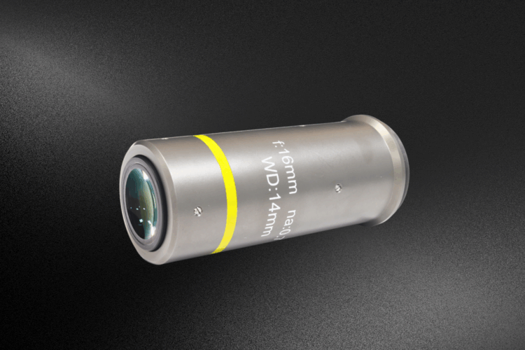
Key Takeaways This case study examines the high NA infinity conjugate long working distance microscope objective, designed for optical tweezers and other precision applications. With a 16 mm focal length, 14 mm working distance, and 0.7 NA, this objective balances resolution and depth. Covering wavelengths from 420-900 nm, it supports various laser sources. The lens corrects for a 3 mm quartz window and requires precise machining due to high sensitivity to tolerances.  Performance testing ensures optimal imaging by adjusting eccentricity and air gaps. Overview of Optical Tweezers Technology  Optical tweezer technology is a tool that utilizes highly focused laser beams to capture and manipulate tiny particles, such as cells and nanoparticles. This technology generates force through the transfer of light, enabling non-contact control of small objects. The focused laser beam creates a strong gradient field near its focal point, attracting tiny particles to the region with high light intensity and thus facilitating capture.  Optical tweezers can manipulate nano-scale particles without causing physical damage to the samples and have demonstrated promising applications across various fields. To achieve effective particle capture in atom capture experiments, lasers typically need to converge to the micron level. Therefore, the microscope objective used in optical tweezer systems must possess high resolution. Increasing the numerical aperture (NA) is one useful method for obtaining high-resolution objective lenses. Since the samples for atom capture experiments are often placed in a vacuum chamber, the microscope objective must also provide a long working distance.  In recent years, microscope objective developers have focused on achieving both high NA and long working distances. High NA microscope objectives are extensively employed in fields such as biology, materials science, and semiconductor detection due to their high resolution and light-gathering ability. Generally, microscope objectives with high NA have shorter working distances. Achieving both high NA and long working distances necessitates the correction of numerous higher-level aberrations during the design phase, leading to complex structures, larger sizes, increased sensitivity to tolerances, and significant design and production challenges. Description of the High NA Objective This specific high NA microscope objective features a numerical aperture of 0.7 and a working distance of 14 mm, resulting in a larger diameter than conventional objectives. Its wide working band, which covers wavelengths from 420 nm to 900 nm, makes it versatile for different laser sources. It is important to note that this objective is designed to correct a quartz window with a thickness of 3 mm; any deviation from this thickness during actual use may diminish the performance of the objective. Working distance is the distance between the observed or processed object and the front end of the lens.  In practical applications, taking into account working distance is crucial when selecting a microscope objective. Typically, a longer working distance offers greater flexibility in application. However, for a fixed NA, increasing the working distance necessitates a larger lens size, while also increasing advanced aberrations within the optical path and complicating the manufacturing process. Additionally, a smaller ratio of focal length to working distance can result in increased spherical error from the rear lens due to the expansion of the optical path aperture, further complicating design efforts. Taking all this into account, the lens is designed with a focal length closely matching the working distance, which is 16 mm, and exhibits low magnification. Specification of the NA0.7 infinitely conjugated long working distance microscope objective Focal length 16mm NA 0.7 Wavelength 420-900nm FOV Φ0.5mm Working distance 14mm(including 3mm fused silica) NA0.7 Infinite conjugate long working distance microscope objective design structure Spot and WFE performance Performance Criteria of the Microscope Objective  The performance of the microscope objective is evaluated based on the size of the dispersion spot and the trans-wavefront error. The design value for the spot radius along the optical axis of this lens is less than 0.4 µm, indicating effective spot convergence at the micron level. Analysis of the transmit-wavefront diagram shows that this objective achieves diffraction-limited performance across various wavelengths, although the off-axis performance slightly exceeds the diffraction limit at 421 nm. Focal shift curve Chromatic Aberration and Wavelength Range  One unique feature of this lens is its operation across a wide range of wavelengths, from violet to near-infrared. Although the correction of chromatic aberration does not meet the diffraction limit, this objective lens has been specifically designed to perform well with laser sources. Only minimal post-focusing adjustments are required when using different light sources, helping to mitigate performance degradation caused by chromatic aberration. For the 421 nm band, the transmission wavefront design performance after focusing is as follows. transmission wavefront error@421nm Design Summary of High NA and Long Working Distance Microscope Objective Lenses The magnification of this micro objective lens is low, approximately 12X when paired with a 200 mm tube lens. The numerical aperture is significant, reaching 0.7, and the working distance extends to 14 mm, with correction for a 3 mm thick quartz window. The objective operates across a broad range of wavelengths from 421 to 900 nm, is compatible with various laser sources, and represents a special type of high-end objective. Optical Component Machining  Given the specific parameters of this objective lens, the effect of tolerance is highly sensitive, requiring precise machining tolerance for all components. The high NA and long working distance further heighten the challenges associated with manufacturing such optical components.  A frame for adjusting this micro objective lens Objective Focusing and Performance Testing  When adjusting the micro objective lens, it is essential to obtain an image of the object and adjust the lens’s eccentricity and air gap based on the imaging results. This process helps eliminate coma and spherical aberration that may arise from manufacturing deviations. The objective in question is a low-magnification microscope lens with a high numerical aperture (NA) and a large entrance pupil. When used with a standard microscope frame, the imaging results may be inadequate, making proper adjustment challenging. To ensure optimal performance, it is important to align the microscope with the object being observed. Measurement Graph: MTF vs. Frequency Customize

Read more
 Laser World of Photonics 2025

Join Avantier at the Laser World of Photonics for an exciting exhibition! Date: June 24-27, 2025 | Booth: Hall B1-171B Location: Trade Fair Center Messe München, Munich, Germany (Map) We are excited to welcome you to our booth, where you can explore our innovative optical solutions. Don’t miss out on exclusive giveaways!  Our team is looking forward to discussing the latest advancements in our products and services, and how they can enhance your projects and help you achieve your goals. To discuss your upcoming projects with us, please schedule an appointment using the form below or click this Google Form link. For further trade show details, please click here (the Laser World of Photonics website). Loading… Featured Products

Read more
Semiconductor Lens Assembly Solutions

Key Takeaways Semiconductor manufacturing requires high-precision optical lens assemblies.  Custom objectives face challenges like miniaturization, thermal instability, and cost.   Semiconductor lens assembly solutions include advanced fabrication, adaptive optics, and thermally stable materials.   Key design considerations are optical performance (NA, chromatic correction, FOV), material selection (low dispersion, high transmittance), and specialized coatings.   Meeting these demands requires a collaborative approach and cutting-edge manufacturing to ensure reliable performance in harsh fab environments. In today’s rapidly advancing technological landscape, semiconductor manufacturing pushes the boundaries of precision and miniaturization. Custom objectives, essential optical components within sophisticated imaging systems, are at the heart of this progress, enabling. These intricate optical lens assemblies enable critical processes like photolithography, wafer inspection, and metrology. This summary delves into optical design considerations for these custom optical systems, exploring the challenges and highlighting innovative assembly solutions. From high NA microscope objectives to complex multi-element lenses, achieving optimal system performance requires careful attention to optical performance, material selection, coating requirements, and robust manufacturing capabilities. Microchip semiconductor manufacturing Design Considerations for Custom Objectives: When designing custom objectives for semiconductor manufacturing and inspection, there are three areas that need special attention: optical performance, materials selection, and coating requirements. Optical PerformanceKey parameters include: Numerical Aperture (NA): High NA (often >0.95) is essential for sub-wavelength resolution. Chromatic Correction: Objectives must perform consistently across multiple wavelengths (e.g., DUV, EUV). Field of View (FOV): Balancing high resolution with a wide FOV is crucial for throughput. Aspheric or freeform lenses may be required. Material Selection:Materials must exhibit: Low Dispersion: Minimizes chromatic aberration. High Transmittance: Maximizes light throughput, especially in UV/DUV. Environmental Stability: Resistance to temperature variations, chemicals, and radiation. Examples include fused silica and CaF2. Coating Requirements:Essential coatings include: Anti-Reflection (AR): Minimizes light loss and enhances contrast. Hard Coatings: Protect lens surfaces from damage. Bandpass Filters: Isolate specific wavelengths for metrology and inspection. Challenges and Solutions: Miniaturization, thermal stability, cost, and environmental challenges can complicate the design process and require carefully crafted solutions. Miniaturization and Complexity: Smaller devices require increasingly complex lens assembly designs and tighter tolerances. Challenge: Achieving nanometer-level accuracy in lens alignment and managing higher-order aberrations in high-NA systems. Solution: Adaptive optics, freeform lens technologies, and advanced fabrication techniques (e.g., diamond turning, computer-controlled polishing). Thermal Stability: Semiconductor environments experience thermal fluctuations that can degrade lens performance. Challenge: Maintaining optical performance despite temperature variations. Solution: Thermally stable materials (e.g., fused silica, ULE glass), athermal designs, and active cooling systems. Cost Considerations: Developing high-end custom objectives is expensive, especially for low-volume production. Challenge: Balancing performance with cost effective solutions. Solution: Collaborative development with optical suppliers, standardized modular designs, and rapid prototyping. Environmental Challenges: Semiconductor fabs present harsh environments with contaminants, vibrations, and chemicals. Challenge: Protecting lenses from these factors. Solution: Protective coatings, vibration isolation systems, and purge systems can maintain a clean optical path. The Future of Semiconductor Lens Assembly Solutions Designing custom objectives for semiconductor applications demands a multifaceted approach, taking into account the complex interplay of optical, material, and environmental factors. Continuous innovation in design, fabrication, and environmental control is necessary in order to meet the stringent quality standards and performance requirements of this industry. Addressing the challenges posed by miniaturization, thermal instability, cost constraints, and harsh environments requires a collaborative effort, leveraging the expertise of a skilled engineering team with advanced manufacturing capabilities.  Optical advances such as  active alignment techniques and a wider range of optical lens assembly types are crucial for ensuring the reliable performance of optical systems in semiconductor manufacturing. Avantier, an ISO 9001 certified company, offers high NA microscope objectives and customized solutions with cutting-edge technologies, manufactured and tested to the highest quality standards. Contact us today for your next project in semiconductors or any other industry that requires high-performance optical systems.  Related Content

Read more
The Critical Role of Custom Objectives in Semiconductor Manufacturing

Key Takeaways Custom optical objectives, especially those with high NA, are crucial for advanced semiconductor manufacturing.  These objectives enable precise photolithography, metrology, and defect inspection for sub-5nm nodes.  While offering high precision, improved yields, and enhanced resolution,  custom  optics also pose challenges in design, manufacturing, and cost.  Emerging trends like meta-lenses and AI-assisted design are driving further innovation. Custom optical objectives are crucial for semiconductor manufacturing and inspection, enabling the precision needed for advanced technologies. High numerical aperture (NA) objectives are particularly important for achieving the resolution required for sub-5nm feature sizes. The semiconductor industry relies heavily on a complex and interconnected supply chain to deliver the cutting-edge products and systems that power modern devices. Within this ecosystem, specialized companies that focus on the design and manufacture of high-precision optical components play a crucial role. Key Applications Photolithography: High NA objectives focus UV or EUV light onto wafers with nanometer precision, creating intricate circuit patterns. They require high transmission at specific wavelengths (e.g., 193nm or 13.5nm), exceptional thermal stability, and minimized aberrations. Metrology and Inspection: Custom objectives can enhance tools like CD-SEMs, optical profilometers, and defect inspection systems. High NA lenses improve resolution and depth of field for precise dimensional measurements and sub-nanometer defect detection. Laser-Based Processes: Custom-built objectives ensure accurate beam focus and uniform energy distribution. They also mitigate thermal damage in applications like laser annealing, drilling, and patterning. Wafer inspection in the semiconductor manufacturing process Challenges in Design Designing a custom objective for specific applications is  a complex process. Thermal stability is often of paramount importance due to the heat generated by high-power light sources. Precision manufacturing is essential, as even minor imperfections can degrade performance. Material selection is critical for optimal transparency and minimal birefringence at specific wavelengths. Cost and time constraints may also pose significant hurdles. Advantages of Custom Objectives: Given numerous design and manufacturing challenges, why choose custom objectives?  A custom-designed and manufactured objective can provide significant performance improvements, and you’re likely to see a number of advantages as you incorporate these objectives into your system: High Precision and Accuracy: Sub-nanometer accuracy is achievable, enabling features down to 5nm and below to be patterned or inspected. Aberration correction can be optimized. Improved Yield and Defect Detection: Early defect detection and precise overlay control lead to high yields in advanced semiconductor nodes. Enhanced Resolution: High NA lenses enable smaller feature sizes for EUV lithography and nanometer-scale defect detection. Thermal Stability and Environmental Control: Low-expansion materials and controlled environments ensure consistent performance across a wide range of temperatures and environmental conditions. Flexibility and Tailored Solutions: Custom designs,  including unique substrates, geometries, and manufacturing processes, meet the needs of specific applications. Supporting Advanced Technologies: Integration of meta-lenses and AI-assisted design further improves performance. Limitations of Custom Objectives: Although custom objectives are invaluable for many semiconductor manufacturing and inspection applications, they do have their downsides. Limitations of custom objectives include: High Costs: Design, prototyping, and testing are expensive and time-consuming. Manufacturing Complexity: Precise alignment during assembly is challenging. Long Development Time: Extended design and manufacturing time impact time-to-market. Limited Scalability: Custom optics often have a high per-unit cost due to low production volumes. Maintenance: Specialized maintenance and servicing are typically required for made-to-order optics. Material Limitations: Finding suitable materials for high-NA objectives under extreme conditions can be challenging. Contamination Sensitivity: EUV systems are highly sensitive to contamination. High NA Systems in Semiconductor Applications High NA objectives are essential for: EUV Lithography: Achieving sub-5nm feature sizes for advanced nodes. Defect Detection: Detecting critical sub-nanometer defects. Metrology Tools: Analyzing surface and subsurface features. Emerging Trends: Meta-Lens Integration: Ultra-thin, high performance systems. AI-Assisted Design: Accelerating development through optimized design parameters. Sustainability: Energy efficiency and environmentally friendly materials. Advanced Node Technology: Enabling next-generation nodes. Photonics for Semiconductors: Driving efficiencies in various processes. Avantier’s High NA Solutions for Semiconductor Applications Custom objectives, particularly high NA systems, are indispensable for semiconductor manufacturing and inspection. Cutting edge optical research promises further advancements, enabling the optics industry to fully meet the evolving demands for semiconductor technology. Avantier’s products and services are specifically tailored to meet the exacting demands of this dynamic industry, providing the critical optical solutions needed for leading-edge semiconductor manufacturing and inspection equipment. We offer high NA microscope objectives and customized solutions with  state-of-the-art technologies.  Contact us today to discuss your next projects and find out more about how we can partner with you. Related Content

Read more
Case Study – UV Microscope Objectives for Genetic Analysis

Key Takeaways A global leader in agricultural genetics sought durable, cost-effective UV microscope objectives.  Challenges included optical design complexity, wavefront control, and fabrication precision.  By optimizing coatings, manufacturing, and materials, we extended the lens lifespan from 3 to 18 months, reducing replacement costs and downtime.  Avantier’s customized optical coatings improved both performance and durability, ensuring reliable genetic analysis. This collaboration set a new standard for high-performance, cost-efficient UV microscope objectives in genetics and reproduction. Project Background:  UV Microscope Objectives for Genetic Analysis A global leader in agricultural genetics and reproduction services approached us to address problems they were facing related to the cost and durability of microscope objective lenses. These lenses play a pivotal role in analyzing genetic data, directly impacting the company’s efficiency and operational costs. By partnering with us, they hoped to enhance the performance and longevity of their UV microscope objectives. Challenges in Designing and Manufacturing UV Microscope Objectives Optical Design Complexity Designing UV microscope objectives involves navigating the unique properties of UV light, such as shorter wavelengths, higher photon energy, and lower transmittance. Advanced optical design techniques needed to be employed to deliver optimal imaging across the entire field of view. One aspect of this was the development of apochromatic equation systems to correct chromatic and spherical aberrations. Material Selection and Manufacturing Processes UV-grade fused silica, prized for its high damage threshold and minimal scattering properties, was selected as the primary substrate. A specialized process was implemented during manufacturing to ensure the highest levels of cleanliness and mitigate potential contamination that could compromise imaging quality. Wavefront Aberration Control Maintaining wavefront aberration below λ/5 across the full wavelength range was crucial for achieving high-resolution, low-distortion imaging. This required meticulous optimization in both the design and manufacturing stages. Precision Fabrication and Testing The high photon energy associated with UV light demands exceptional surface quality and precision in optical components. Advanced fabrication techniques, coupled with state-of-the-art metrology technologies, were employed to meet these exacting requirements. Cost and Efficiency Challenges High production costs traditionally limit the widespread adoption of UV microscope objectives. Addressing this, we focused on reducing manufacturing expenses while maintaining stringent quality standards and optimizing production efficiency. Solutions and Outcomes Customized Optical Coatings To meet the company’s specific needs, a customized optical coating solution was developed in collaboration with Avantier. These coatings enhanced the durability and performance of the microscope objectives, enabling them to withstand the demanding conditions under which they were used.  Significant Longevity Improvements Through the implementation of advanced materials, coatings, and precision manufacturing processes, the operational lifespan of the UV microscope objectives was extended from 3 months to 18 months—a sixfold increase in durability.  Cost and Time Savings The extended longevity of the lenses drastically reduced the frequency of replacements, leading to substantial cost savings and minimized instrument downtime. This improvement streamlined the operations of the genetic analysis company, enabling them to allocate resources more effectively. UV Microscope Objectives for Genetic Analysis Enhancing UV Microscope Objectives  By addressing the complexities of UV light, selecting the best materials, and employing cutting-edge manufacturing techniques, we successfully delivered a robust solution that exceeded our client’s expectations. The collaboration not only resolved their immediate challenges but also set a new benchmark for cost-efficient, high-performance UV microscope objectives in the field of genetics and reproduction. Please contact us if you’d like to request a quote on your next project. Related Content

Read more
Athermal Design and Manufacturing

Key Takeaways: Athermal Design ensures stable performance of athermal optical systems across a wide temperature range. Athermalization techniques minimize the impact of temperature fluctuations on imaging quality. Careful material selection and advanced optical design are crucial for successful athermalization. Athermal optical systems find applications in diverse fields, including aerospace, defense, and medical imaging. Athermal Optics Masters Temperature Challenges Athermal optical systems are engineered to maintain consistent performance across a wide range of temperatures without the need for active thermal compensation. This is crucial for applications like aerospace, defense, and outdoor imaging where environmental conditions can fluctuate dramatically. By eliminating the need for complex thermal controls, athermal designs offer enhanced reliability and performance under extreme conditions. Maintaining optical precision across extreme temperatures. An athermal optical system designed for challenging environments. Key Characteristics Passive Thermal Compensation: Athermal systems utilize materials and configurations that automatically adjust to temperature-induced changes, ensuring stable optical performance. Wide Temperature Range: These systems operate efficiently across a broad temperature spectrum, typically from -40°C to +80°C or more. Material Selection: Careful selection of materials with specific thermal expansion coefficients (CTE) and refractive index temperature dependencies is essential for maintaining optical stability. Athermal Design Principles When designing an athermal optical system, both application-specific requirements and general athermalization techniques  must be kept in mind. Some important aspects of athermal design include: Thermal Compensation: Athermal designs combine materials with complementary thermal properties. For example, high dn/dT (refractive index change with temperature) materials like Germanium are paired with low dn/dT materials such as Zinc Sulfide or Calcium Fluoride to balance thermal-induced focal shifts. To maintain system effectiveness over a wide range of wavelengths, only substrates which stay transparent over the entire relevant temperature range may be used.  Optical Layout: Advanced optical components like achromatic doublets and aspheric surfaces are employed to counteract thermal effects and enhance overall performance. Mechanical Design: Low-expansion alloys like Invar are used for mounts and housings to minimize distortion and prevent misalignment due to temperature variations. Design Process Some processes important to the design of athermal  design include: Temperature Modeling: Advanced simulation software is used to model temperature effects on optical performance, allowing designers to anticipate potential issues early in the development process. Material Selection: Identifying materials with complementary CTEs and thermo-optic coefficients is crucial for ensuring system thermal stability. Athermal Optimization: Software like Zemax or Code V is used to fine-tune the design, optimizing the layout for both performance and manufacturability. Tolerance analysis is also performed to ensure the system meets stringent production requirements. Manufacturing Considerations Material Precision: Materials like Germanium and Zinc Sulfide are sensitive to thermal and mechanical stresses, requiring precise fabrication techniques like diamond turning to maintain high levels of accuracy and minimize defects. Coating: Applying anti-reflective (AR) coatings designed specifically for infrared wavelengths (3–5 µm or 8–12 µm) is vital for maintaining performance. These coatings must withstand the stresses of thermal cycling, and may require advanced application techniques to ensure durability and adhesion. Lens Surface Quality: Maintaining high-quality lens surfaces is critical. Stringent scratch-dig specifications are enforced to ensure minimal scattering and achieve clear, sharp imaging. Mechanical Housing: Housings made from materials like Invar or Titanium, which have low thermal expansion coefficients, are carefully designed to ensure that components remain securely aligned under varying temperature conditions. Testing Methodologies: After manufacturing, each athermal system is subjected to thorough testing to ensure it will perform as expected over the entire relevant temperature range. Environmental Stress Testing: Thermal cycling tests, which subject the system to temperatures ranging from -40°C to +85°C, simulate real-world environmental conditions. Vibration testing is also conducted to ensure system stability during transportation or deployment in rugged environments. Optical Performance Testing: Modulation Transfer Function (MTF) measurements are taken across temperature ranges to verify that the system meets performance standards and that the image remains clear and sharp. Coating Verification: The durability and performance of AR coatings are rigorously tested using spectrophotometry to ensure they provide reliable transmission and resist degradation under thermal stress. Reliability Testing: Long-term exposure to thermal and mechanical stress is used to ensure the system will maintain its performance and structural integrity over time. Advantages of Athermal Optics There are many benefits to using athermal optics when working under high or changing temperatures. A few of them include: Thermal Stability: Athermal designs ensure that optical systems deliver consistent performance, even in harsh environmental conditions. Reduced Maintenance: The passive nature of athermal systems eliminates the need for complex active compensation mechanisms, leading to lower maintenance costs. Improved Imaging Performance: By compensating for thermal effects, athermal optics deliver clear, high-resolution images with minimal distortion, even in extreme conditions. Compact Designs: Athermal systems can achieve smaller, lighter designs by reducing the number of components, making them more efficient and easier to integrate into various applications. Challenges Despite their benefits, developing and deploying athermal optics involve several challenges that require advanced techniques and innovative approaches to overcome: Material Machining: The brittleness of materials like Germanium and Zinc Sulfide requires careful machining techniques like diamond turning to minimize damage. Coating Application: Ensuring that AR coatings adhere uniformly to the materials is challenging. Advanced deposition techniques are employed to enhance durability. Alignment Precision: Achieving perfect alignment during assembly is crucial for system performance. Advanced alignment tools and stress-free mounting techniques are utilized. Thermal Stress Management: Managing thermal stress from mismatched CTEs can lead to mechanical issues. Selecting materials with complementary CTEs and using thermal compensators are crucial to high performance in athermal systems. Testing and Quality Assurance: Comprehensive testing is resource-intensive. Automating testing processes and implementing rigorous quality control protocols are essential. Cost and Scalability: Manufacturing athermal systems can be expensive. Optimizing designs, streamlining processes, and exploring partnerships are crucial to lower costs. While athermal optics excel at addressing thermal challenges, limitations in material selection, environmental factors, and manufacturing costs underline the importance of balancing their benefits with practical constraints. Athermal Optics for Superior Imaging Athermal optics are a transformative technology, ensuring that optical systems perform reliably across a wide range of environmental conditions, from extreme

Read more
Athermal Optical Systems

Key Takeaways Athermal optical systems leverage sophisticated athermalization techniques, advanced materials like ALLVAR Alloy 30, and precise designs to maintain performance under temperature changes.  These systems are essential in infrared imaging, space optics, and telecommunications.  Innovations such as passive athermalization and uncooled detectors enhance their versatility.  Despite material constraints and design challenges, athermal optical systems deliver reliable, cost-effective solutions for precision applications. What are Athermal Optical Systems? Athermal optical systems are a cornerstone of modern optics, designed to ensure consistent optical performance across varying temperatures. These systems are indispensable in environments where precision and reliability are non-negotiable.  Principles of Athermalization Athermalization involves a combination of optical, mechanical, and material strategies to counteract the effects of temperature changes on optical systems. The key principles include: Material SelectionChoosing the right materials is fundamental to passive athermalization. Optical Materials: Glasses with low thermal expansion and complementary dn/dT values help counteract temperature effects. Housing Materials: Innovative materials like ALLVAR Alloy 30, with a negative CTE, expand design possibilities. Optical Design StrategiesCareful optical design ensures temperature stability without compromising performance. Achrothermic Systems: Dual optimization for achromatic and athermal properties enhances system stability. Wavefront Aberration Theory: Designs are refined to minimize aberrations caused by temperature changes. Mechanical Design TechniquesMechanical adjustments play a critical role in maintaining stability. Passive Athermalization: Design housing components to compensate for thermal expansion of optical elements. Bimetallic Housings: Combining materials with different thermal properties achieves optimal results. Mathematical ModelingPrecise equations and modeling ensure accurate compensation for thermal effects. Thermal ν-number and CTD can be used to calculate and correct focal shifts due to temperature variations. Index MatchingSynchronizing refractive index changes and thermal expansion ensures seamless performance. This technique enhances reliability but can add design complexity. The focal length of a lens shifts due to temperature changes that alter the refractive index and the lens’s position Advantages of Athermal Systems Athermal systems excel in maintaining performance across extreme temperature ranges. But the benefits of athermal systems extend beyond temperature stability. Other advantages you are likely to see include: Reliability: With fewer active components, athermal systems are robust and require less maintenance. Cost-Effectiveness: Passive designs eliminate the need for energy-intensive thermal controls, making them ideal for challenging environments. Limitations Despite their advantages, athermal systems face inherent challenges that demand innovative solutions. Design Complexity: Developing athermal systems requires advanced techniques and extended timelines. Performance Trade-offs: Prioritizing thermal stability may impact other optical properties. Environmental Sensitivity: While effective against temperature changes, these systems can still be influenced by factors like humidity or pressure. Applications The versatility of athermal optical systems makes them indispensable across diverse industries. Infrared Imaging: Essential in thermal cameras, where maintaining focus is critical for security and surveillance. Space Optics: Power-efficient and reliable, they are well suited to the extreme conditions of space exploration. Industrial Monitoring: Their robustness ensures consistent performance in high-temperature environments, such as furnaces and chemical plants. Telecommunications: Athermal designs enhance fiber coupling efficiency, something that is critical for WDM systems. Recent Developments Continuous innovation is expanding the horizons of athermal optical systems. Expanded Materials: Research into materials with a negative coefficient of thermal expansion, such as ALLVAR Alloy 30, is broadening possibilities for athermal optical designs. Passive Athermalization: Collaboration between industry leaders has improved the performance of commercially available optical doublets. Technological Integration: Advances in uncooled detectors and wafer-scale manufacturing enhance the accessibility and affordability of athermal systems. Design Challenges and Solutions Designing athermal systems such as infrared optics requires overcoming significant technical obstacles, including material and thermal limitations. Material Limitations: The need for unique thermal properties, combined with optical requirements, narrows available options. Thermal Defocus: Addressing focal shifts due to temperature requires precision modeling. Solutions: Advanced materials and glass maps optimize design for both lens and housing. Integrated optical-thermal analysis anticipates potential misalignments and thermal effects. Techniques like wavefront aberration optimization enable consistent performance across varying temperatures. The Future of Athermal Optical Systems Athermal optical systems are at the forefront of research in  optical designs, as we discover new and better ways to deliver stability and reliability in diverse and challenging environments. As innovation in materials and design continues, these systems are poised to play a pivotal role in advancing industries like space exploration, telecommunications, and industrial monitoring. Their ability to adapt and perform under extreme conditions makes them an invaluable asset in modern optics. Contact us  on your athermal optics project. Related Content

Read more