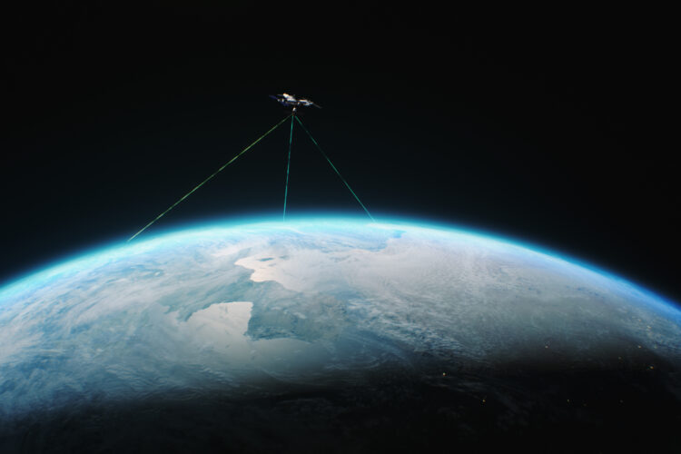
Optical Glass Comparative Table

Optical glass is utilized in a wide range of optical devices, including DSLR cameras, automotive cameras, security cameras, medical equipment, and others. Optical Glass Comparative Table Choosing the right type of glass material is crucial, as different types exhibit various properties. Avantier offers a selection of glass types based on the following characteristics: The table below lists the codes and equivalent glass type names for Avantier, SCHOTT, OHARA, HOYA, and CDGM. The codes are composed of six digits, where the first three digits represent the refractive index (nd), and the last three digits denote the Abbe number (νd). Material Equivalency List Avantier Code Schott Avantier Code2 Ohara Avantier Code3 Hoya Avantier Code4 CDGM — — 439-950 S-FPL53 — — — — — — — — 457-903 FCD10 457-903 H-FK71 471-673 FK1 471-674 FSL1 471-673 FC1 470-668 H-QK1 487-704 N-FK5 487-702 S-FSL5 487-704 FC5 487-704 H-QK3L 487-845 N-FK51A — — — — — — 497-816 N-PK52A 497-816 S-FPL51 497-816 FCD1 497-816 H-FK61 498-670 N-BK10 — — — — — — 500-658 BK4 500-660 BSL4 500-660 BSC4 500-660 H-K2 501-564 K10 — — — — — — — — — — 505-650 BK5 505-647 H-K3 508-612 N-ZK7 508-608 ZSL7 508-613 ZNC7 508-611 K4A 510-635 BK1 510-636 BSL1 510-634 BSC1 510-634 H-K5 511-604 K7 511-605 NSL7 511-605 C7 511-605 H-K6 — — — — — — 515-606 H-K7 517-642 N-BK7 516-641 S-BSL7 517-642 BSC7 517-642 H-K9L — — 517-524 S-NSL36 517-522 E-CF6 517-522 H-KF6 — — 518-590 S-NSL3 518-590 E-C3 518-590 H-K10 — — — — — — 518-635 D-K59 522-595 N-K5 522-598 S-NSL5 522-595 C5 522-592 H-K50 523-515 N-KF9 — — — — — — — — 523-585 NSL51 523-586 C12 523-586 H-K51 — — — — — — 525-704 D-PK3 526-600 BALK1 526-600 NSL21 526-601 BACL1 526-602 H-K11 529-770 N-PK51 — — — — — — — — — — — — 530-605 H-BaK1 531-488 LLF6 532-489 PBL6 532-488 FEL6 532-488 QF6 532-489 N-LLF6 532-489 S-TIL6 532-488 E-FEL6 532-488 H-QF6A 540-597 N-BAK2 540-595 S-BAL12 540-597 BAC2 540-597 H-BaK2 541-472 LLF2 541-472 PBL2 541-472 FEL2 541-472 QF8 — — 541-472 S-TIL2 541-472 E-FEL2 541-472 H-QF8 547-536 N-BALF5 — — — — — — 548-458 N-FEL1 548-458 S-TIL1 548-458 E-FEL1 548-458 H-QF1 548-458 LLF1 548-458 PBL1 548-458 FEL1 548-459 QF1 — — — — 548-628 BAL21 547-628 H-BaK3 552-635 N-PSK3 552-638 BAL23 552-634 PCD3 552-634 H-BaK4 558-540 N-KZFS2 — — — — — — — — — — — — 561-583 H-BaK5 564-608 N-SK11 564-607 S-BAL41 564-608 BACD11 564-608 H-BaK6 — – 567-428 S-TIL26 567-428 E-FL6 567-428 H-QF56 569-560 N-BAK4 569-563 S-BAL14 569-560 BAC4 569-560 H-BaK7 569-631 PSK2 569-631 BAL22 569-631 PCD2 569-629 H-ZK1 570-494 BAF2 570-493 BAM2 570-492 BAF2 570-495 BaF2 — — 571-508 S-BAL2 — — — — — — 571-530 S-BAL3 — — — — 573-576 N-BAK1 573-575 S-BAL11 573-575 BAC1 573-575 H-BaK8 575-415 LF7 575-415 PBL27 575-413 FL7 575-413 QF3 — — 575-415 S-TIL27 — — 575-415 H-QF3 580-539 N-BALF4 — — 580-539 N-BALF4 580-537 H-BaF3 581-409 LF5 581-407 PBL25 581-409 FL5 581-409 QF50 581-409 N-LF5 581-407 S-TIL25 581-409 E-FL5 581-409 H-QF50 582-421 LF3 582-421 PBL23 582-420 FL3 582-420 QF5 — — 583-464 S-BAM3 — — — — 583-595 SK12 583-594 S-BAL42 583-595 BACD12 583-595 H-ZK2 — — 583-594 L-BAL42 583-595 M-BACD12 583-594 D-ZK2 589-613 N-SK5 589-612 S-BAL35 589-613 BACD5 589-613 H-ZK3 589-612 P-SK58A 589-612 L-BAL35 589-613 M-BACD5N 589-612 D-ZK3 — — 593-353 S-FTM16 593-355 FF5 — — — — 595-677 S-FPM2 — — — — — — 596-392 S-TIM8 596-392 E-F8 596-392 H-QF14 603-380 F5 603-380 PBM5 603-380 F5 603-380 F1 — — 603-380 S-TIM5 603-380 E-F5 603-380 H-F1 603-606 N-SK14 603-607 S-BSM14 603-607 BACD14 603-606 H-ZK14 — — 603-655 S-PHM53 — — 603-655 H-ZPK2 606-437 BAF4 606-437 BAM4 606-439 BAF4 606-439 BaF5 606-437 N-BAF4 606-437 S-BAM4 — — — — — — — — 606-637 LBC3N — — 607-567 N-SK2 607-568 BSM2 607-567 BACD2 607-567 H-ZK50 — — 607-568 S-BSM2 — — — — — — — — 608-462 BAF7 608-462 H-BaF6 609-466 N-BAF52 — — — — — — — — — — — — 609-579 D-ZK79 609-589 SK3 609-590 BSM3 609-589 BACD3 609-589 H-ZK4 611-559 SK8 611-559 BSM8 611-558 BACD8 611-558 H-ZK50 613-370 F3 613-370 PBM3 613-370 F3 613-370 F2 — — 613-370 S-TIM3 613-370 E-F3 613-370 H-F2 613-443 KZFS4 613-442 BPM51 613-443 ADF40 612-441 TF3 — — 613-443 S-NBM51 — — 613-441 H-TF3L 613-445 N-KZFS4 — — — — — — 613-586 N-SK4 613-587 S-BSM4 613-586 BACD4 613-586 H-ZK6 — — — — — — 613-606 H-ZK7 — — — — — — 614-400 BaF7 — — — — 613-444 E-ADF10 — — 614-552 SK9 614-550 S-BSM9 614-551 BACD9 614-551 H-ZK8 617-366 F4 617-366 PBM4 617-366 F4 617-366 F3 617-539 SSK1 617-540 BSM21 617-539 BACED1 617-539 H-ZK20 618-498 N-SSK8 618-498 S-BSM28 — — — — 618-634 N-PSK53A 618-634 S-PHM52 618-634 PCD4 618-634 H-ZPK1 620-364 F2 620-363 PBM2 620-363 F2 620-364 F4 620-364 N-F2 620-363 S-TIM2 620-363 E-F2 620-364 H-F4 620-603 N-SK16 620-603 S-BSM16 620-603 BACD16 620-603 H-ZK9B — — — — 620-622 ADC1 — — — — — — 621-359 PBM11 624-359 F5 622-533 N-SSK2 622-532 S-BSM22 — — 622-532 H-ZBaF1 — — — — — — 622-567 H-ZK10 622-570 N-SK10 623-570 S-BSM10 623-569 E-BACD10 623-569 H-ZK10L 623-580 N-SK15 623-582 S-BSM15 623-581 BACD15 623-581 H-ZK21 — — — — 624-471 E-BAF8 — — — — — — 625-356 F7 625-356 F6 — — 626-357 S-TIM1 626-357 E-F1 626-357 H-F13 626-357 F1 626-357 PBM1 626-375 F1 626-357 F13 626-390 BASF1 626-392 BAM21 626-391 BAFD1 626-391 H-BaF8 636-353 F6 636-354 PBM6 636-353 F6 636-354 F7 638-424 N-KZFS11 — — — — — — — — 639-449 S-BAM12 — — — — 639-554 N-SK18 639-554 S-BSM18 639-555 BACD18 639-555 H-ZK11 — — 640-354 S-TIM27 640-354 E-FD7 640-354 H-F51 — — — — — — 640-483 ZBaF2 640-601 N-LAK21 640-601 S-BSM81 640-602 LACL60 640-602 H-LaK4L 648-339 SF2 648-338 PBM22 648-338 FD2 648-338 ZF1 648-338 N-SF2 648-338 S-TIM22 648-338 E-FD2 648-338 H-ZF1 — — 649-530 S-BSM71 649-530 E-BACEED20

Read more
Semiconductor Lens Assembly Solutions

Key Takeaways Semiconductor manufacturing requires high-precision optical lens assemblies.  Custom objectives face challenges like miniaturization, thermal instability, and cost.   Semiconductor lens assembly solutions include advanced fabrication, adaptive optics, and thermally stable materials.   Key design considerations are optical performance (NA, chromatic correction, FOV), material selection (low dispersion, high transmittance), and specialized coatings.   Meeting these demands requires a collaborative approach and cutting-edge manufacturing to ensure reliable performance in harsh fab environments. In today’s rapidly advancing technological landscape, semiconductor manufacturing pushes the boundaries of precision and miniaturization. Custom objectives, essential optical components within sophisticated imaging systems, are at the heart of this progress, enabling. These intricate optical lens assemblies enable critical processes like photolithography, wafer inspection, and metrology. This summary delves into optical design considerations for these custom optical systems, exploring the challenges and highlighting innovative assembly solutions. From high NA microscope objectives to complex multi-element lenses, achieving optimal system performance requires careful attention to optical performance, material selection, coating requirements, and robust manufacturing capabilities. Microchip semiconductor manufacturing Design Considerations for Custom Objectives: When designing custom objectives for semiconductor manufacturing and inspection, there are three areas that need special attention: optical performance, materials selection, and coating requirements. Optical PerformanceKey parameters include: Numerical Aperture (NA): High NA (often >0.95) is essential for sub-wavelength resolution. Chromatic Correction: Objectives must perform consistently across multiple wavelengths (e.g., DUV, EUV). Field of View (FOV): Balancing high resolution with a wide FOV is crucial for throughput. Aspheric or freeform lenses may be required. Material Selection:Materials must exhibit: Low Dispersion: Minimizes chromatic aberration. High Transmittance: Maximizes light throughput, especially in UV/DUV. Environmental Stability: Resistance to temperature variations, chemicals, and radiation. Examples include fused silica and CaF2. Coating Requirements:Essential coatings include: Anti-Reflection (AR): Minimizes light loss and enhances contrast. Hard Coatings: Protect lens surfaces from damage. Bandpass Filters: Isolate specific wavelengths for metrology and inspection. Challenges and Solutions: Miniaturization, thermal stability, cost, and environmental challenges can complicate the design process and require carefully crafted solutions. Miniaturization and Complexity: Smaller devices require increasingly complex lens assembly designs and tighter tolerances. Challenge: Achieving nanometer-level accuracy in lens alignment and managing higher-order aberrations in high-NA systems. Solution: Adaptive optics, freeform lens technologies, and advanced fabrication techniques (e.g., diamond turning, computer-controlled polishing). Thermal Stability: Semiconductor environments experience thermal fluctuations that can degrade lens performance. Challenge: Maintaining optical performance despite temperature variations. Solution: Thermally stable materials (e.g., fused silica, ULE glass), athermal designs, and active cooling systems. Cost Considerations: Developing high-end custom objectives is expensive, especially for low-volume production. Challenge: Balancing performance with cost effective solutions. Solution: Collaborative development with optical suppliers, standardized modular designs, and rapid prototyping. Environmental Challenges: Semiconductor fabs present harsh environments with contaminants, vibrations, and chemicals. Challenge: Protecting lenses from these factors. Solution: Protective coatings, vibration isolation systems, and purge systems can maintain a clean optical path. The Future of Semiconductor Lens Assembly Solutions Designing custom objectives for semiconductor applications demands a multifaceted approach, taking into account the complex interplay of optical, material, and environmental factors. Continuous innovation in design, fabrication, and environmental control is necessary in order to meet the stringent quality standards and performance requirements of this industry. Addressing the challenges posed by miniaturization, thermal instability, cost constraints, and harsh environments requires a collaborative effort, leveraging the expertise of a skilled engineering team with advanced manufacturing capabilities.  Optical advances such as  active alignment techniques and a wider range of optical lens assembly types are crucial for ensuring the reliable performance of optical systems in semiconductor manufacturing. Avantier, an ISO 9001 certified company, offers high NA microscope objectives and customized solutions with cutting-edge technologies, manufactured and tested to the highest quality standards. Contact us today for your next project in semiconductors or any other industry that requires high-performance optical systems.  Related Content

Read more
The Critical Role of Custom Objectives in Semiconductor Manufacturing

Key Takeaways Custom optical objectives, especially those with high NA, are crucial for advanced semiconductor manufacturing.  These objectives enable precise photolithography, metrology, and defect inspection for sub-5nm nodes.  While offering high precision, improved yields, and enhanced resolution,  custom  optics also pose challenges in design, manufacturing, and cost.  Emerging trends like meta-lenses and AI-assisted design are driving further innovation. Custom optical objectives are crucial for semiconductor manufacturing and inspection, enabling the precision needed for advanced technologies. High numerical aperture (NA) objectives are particularly important for achieving the resolution required for sub-5nm feature sizes. The semiconductor industry relies heavily on a complex and interconnected supply chain to deliver the cutting-edge products and systems that power modern devices. Within this ecosystem, specialized companies that focus on the design and manufacture of high-precision optical components play a crucial role. Key Applications Photolithography: High NA objectives focus UV or EUV light onto wafers with nanometer precision, creating intricate circuit patterns. They require high transmission at specific wavelengths (e.g., 193nm or 13.5nm), exceptional thermal stability, and minimized aberrations. Metrology and Inspection: Custom objectives can enhance tools like CD-SEMs, optical profilometers, and defect inspection systems. High NA lenses improve resolution and depth of field for precise dimensional measurements and sub-nanometer defect detection. Laser-Based Processes: Custom-built objectives ensure accurate beam focus and uniform energy distribution. They also mitigate thermal damage in applications like laser annealing, drilling, and patterning. Wafer inspection in the semiconductor manufacturing process Challenges in Design Designing a custom objective for specific applications is  a complex process. Thermal stability is often of paramount importance due to the heat generated by high-power light sources. Precision manufacturing is essential, as even minor imperfections can degrade performance. Material selection is critical for optimal transparency and minimal birefringence at specific wavelengths. Cost and time constraints may also pose significant hurdles. Advantages of Custom Objectives: Given numerous design and manufacturing challenges, why choose custom objectives?  A custom-designed and manufactured objective can provide significant performance improvements, and you’re likely to see a number of advantages as you incorporate these objectives into your system: High Precision and Accuracy: Sub-nanometer accuracy is achievable, enabling features down to 5nm and below to be patterned or inspected. Aberration correction can be optimized. Improved Yield and Defect Detection: Early defect detection and precise overlay control lead to high yields in advanced semiconductor nodes. Enhanced Resolution: High NA lenses enable smaller feature sizes for EUV lithography and nanometer-scale defect detection. Thermal Stability and Environmental Control: Low-expansion materials and controlled environments ensure consistent performance across a wide range of temperatures and environmental conditions. Flexibility and Tailored Solutions: Custom designs,  including unique substrates, geometries, and manufacturing processes, meet the needs of specific applications. Supporting Advanced Technologies: Integration of meta-lenses and AI-assisted design further improves performance. Limitations of Custom Objectives: Although custom objectives are invaluable for many semiconductor manufacturing and inspection applications, they do have their downsides. Limitations of custom objectives include: High Costs: Design, prototyping, and testing are expensive and time-consuming. Manufacturing Complexity: Precise alignment during assembly is challenging. Long Development Time: Extended design and manufacturing time impact time-to-market. Limited Scalability: Custom optics often have a high per-unit cost due to low production volumes. Maintenance: Specialized maintenance and servicing are typically required for made-to-order optics. Material Limitations: Finding suitable materials for high-NA objectives under extreme conditions can be challenging. Contamination Sensitivity: EUV systems are highly sensitive to contamination. High NA Systems in Semiconductor Applications High NA objectives are essential for: EUV Lithography: Achieving sub-5nm feature sizes for advanced nodes. Defect Detection: Detecting critical sub-nanometer defects. Metrology Tools: Analyzing surface and subsurface features. Emerging Trends: Meta-Lens Integration: Ultra-thin, high performance systems. AI-Assisted Design: Accelerating development through optimized design parameters. Sustainability: Energy efficiency and environmentally friendly materials. Advanced Node Technology: Enabling next-generation nodes. Photonics for Semiconductors: Driving efficiencies in various processes. Avantier’s High NA Solutions for Semiconductor Applications Custom objectives, particularly high NA systems, are indispensable for semiconductor manufacturing and inspection. Cutting edge optical research promises further advancements, enabling the optics industry to fully meet the evolving demands for semiconductor technology. Avantier’s products and services are specifically tailored to meet the exacting demands of this dynamic industry, providing the critical optical solutions needed for leading-edge semiconductor manufacturing and inspection equipment. We offer high NA microscope objectives and customized solutions with  state-of-the-art technologies.  Contact us today to discuss your next projects and find out more about how we can partner with you. Related Content

Read more
Athermal Design and Manufacturing

Key Takeaways: Athermal Design ensures stable performance of athermal optical systems across a wide temperature range. Athermalization techniques minimize the impact of temperature fluctuations on imaging quality. Careful material selection and advanced optical design are crucial for successful athermalization. Athermal optical systems find applications in diverse fields, including aerospace, defense, and medical imaging. Athermal Optics Masters Temperature Challenges Athermal optical systems are engineered to maintain consistent performance across a wide range of temperatures without the need for active thermal compensation. This is crucial for applications like aerospace, defense, and outdoor imaging where environmental conditions can fluctuate dramatically. By eliminating the need for complex thermal controls, athermal designs offer enhanced reliability and performance under extreme conditions. Maintaining optical precision across extreme temperatures. An athermal optical system designed for challenging environments. Key Characteristics Passive Thermal Compensation: Athermal systems utilize materials and configurations that automatically adjust to temperature-induced changes, ensuring stable optical performance. Wide Temperature Range: These systems operate efficiently across a broad temperature spectrum, typically from -40°C to +80°C or more. Material Selection: Careful selection of materials with specific thermal expansion coefficients (CTE) and refractive index temperature dependencies is essential for maintaining optical stability. Athermal Design Principles When designing an athermal optical system, both application-specific requirements and general athermalization techniques  must be kept in mind. Some important aspects of athermal design include: Thermal Compensation: Athermal designs combine materials with complementary thermal properties. For example, high dn/dT (refractive index change with temperature) materials like Germanium are paired with low dn/dT materials such as Zinc Sulfide or Calcium Fluoride to balance thermal-induced focal shifts. To maintain system effectiveness over a wide range of wavelengths, only substrates which stay transparent over the entire relevant temperature range may be used.  Optical Layout: Advanced optical components like achromatic doublets and aspheric surfaces are employed to counteract thermal effects and enhance overall performance. Mechanical Design: Low-expansion alloys like Invar are used for mounts and housings to minimize distortion and prevent misalignment due to temperature variations. Design Process Some processes important to the design of athermal  design include: Temperature Modeling: Advanced simulation software is used to model temperature effects on optical performance, allowing designers to anticipate potential issues early in the development process. Material Selection: Identifying materials with complementary CTEs and thermo-optic coefficients is crucial for ensuring system thermal stability. Athermal Optimization: Software like Zemax or Code V is used to fine-tune the design, optimizing the layout for both performance and manufacturability. Tolerance analysis is also performed to ensure the system meets stringent production requirements. Manufacturing Considerations Material Precision: Materials like Germanium and Zinc Sulfide are sensitive to thermal and mechanical stresses, requiring precise fabrication techniques like diamond turning to maintain high levels of accuracy and minimize defects. Coating: Applying anti-reflective (AR) coatings designed specifically for infrared wavelengths (3–5 µm or 8–12 µm) is vital for maintaining performance. These coatings must withstand the stresses of thermal cycling, and may require advanced application techniques to ensure durability and adhesion. Lens Surface Quality: Maintaining high-quality lens surfaces is critical. Stringent scratch-dig specifications are enforced to ensure minimal scattering and achieve clear, sharp imaging. Mechanical Housing: Housings made from materials like Invar or Titanium, which have low thermal expansion coefficients, are carefully designed to ensure that components remain securely aligned under varying temperature conditions. Testing Methodologies: After manufacturing, each athermal system is subjected to thorough testing to ensure it will perform as expected over the entire relevant temperature range. Environmental Stress Testing: Thermal cycling tests, which subject the system to temperatures ranging from -40°C to +85°C, simulate real-world environmental conditions. Vibration testing is also conducted to ensure system stability during transportation or deployment in rugged environments. Optical Performance Testing: Modulation Transfer Function (MTF) measurements are taken across temperature ranges to verify that the system meets performance standards and that the image remains clear and sharp. Coating Verification: The durability and performance of AR coatings are rigorously tested using spectrophotometry to ensure they provide reliable transmission and resist degradation under thermal stress. Reliability Testing: Long-term exposure to thermal and mechanical stress is used to ensure the system will maintain its performance and structural integrity over time. Advantages of Athermal Optics There are many benefits to using athermal optics when working under high or changing temperatures. A few of them include: Thermal Stability: Athermal designs ensure that optical systems deliver consistent performance, even in harsh environmental conditions. Reduced Maintenance: The passive nature of athermal systems eliminates the need for complex active compensation mechanisms, leading to lower maintenance costs. Improved Imaging Performance: By compensating for thermal effects, athermal optics deliver clear, high-resolution images with minimal distortion, even in extreme conditions. Compact Designs: Athermal systems can achieve smaller, lighter designs by reducing the number of components, making them more efficient and easier to integrate into various applications. Challenges Despite their benefits, developing and deploying athermal optics involve several challenges that require advanced techniques and innovative approaches to overcome: Material Machining: The brittleness of materials like Germanium and Zinc Sulfide requires careful machining techniques like diamond turning to minimize damage. Coating Application: Ensuring that AR coatings adhere uniformly to the materials is challenging. Advanced deposition techniques are employed to enhance durability. Alignment Precision: Achieving perfect alignment during assembly is crucial for system performance. Advanced alignment tools and stress-free mounting techniques are utilized. Thermal Stress Management: Managing thermal stress from mismatched CTEs can lead to mechanical issues. Selecting materials with complementary CTEs and using thermal compensators are crucial to high performance in athermal systems. Testing and Quality Assurance: Comprehensive testing is resource-intensive. Automating testing processes and implementing rigorous quality control protocols are essential. Cost and Scalability: Manufacturing athermal systems can be expensive. Optimizing designs, streamlining processes, and exploring partnerships are crucial to lower costs. While athermal optics excel at addressing thermal challenges, limitations in material selection, environmental factors, and manufacturing costs underline the importance of balancing their benefits with practical constraints. Athermal Optics for Superior Imaging Athermal optics are a transformative technology, ensuring that optical systems perform reliably across a wide range of environmental conditions, from extreme

Read more
Athermal Optical Systems

Key Takeaways Athermal optical systems leverage sophisticated athermalization techniques, advanced materials like ALLVAR Alloy 30, and precise designs to maintain performance under temperature changes.  These systems are essential in infrared imaging, space optics, and telecommunications.  Innovations such as passive athermalization and uncooled detectors enhance their versatility.  Despite material constraints and design challenges, athermal optical systems deliver reliable, cost-effective solutions for precision applications. What are Athermal Optical Systems? Athermal optical systems are a cornerstone of modern optics, designed to ensure consistent optical performance across varying temperatures. These systems are indispensable in environments where precision and reliability are non-negotiable.  Principles of Athermalization Athermalization involves a combination of optical, mechanical, and material strategies to counteract the effects of temperature changes on optical systems. The key principles include: Material SelectionChoosing the right materials is fundamental to passive athermalization. Optical Materials: Glasses with low thermal expansion and complementary dn/dT values help counteract temperature effects. Housing Materials: Innovative materials like ALLVAR Alloy 30, with a negative CTE, expand design possibilities. Optical Design StrategiesCareful optical design ensures temperature stability without compromising performance. Achrothermic Systems: Dual optimization for achromatic and athermal properties enhances system stability. Wavefront Aberration Theory: Designs are refined to minimize aberrations caused by temperature changes. Mechanical Design TechniquesMechanical adjustments play a critical role in maintaining stability. Passive Athermalization: Design housing components to compensate for thermal expansion of optical elements. Bimetallic Housings: Combining materials with different thermal properties achieves optimal results. Mathematical ModelingPrecise equations and modeling ensure accurate compensation for thermal effects. Thermal ν-number and CTD can be used to calculate and correct focal shifts due to temperature variations. Index MatchingSynchronizing refractive index changes and thermal expansion ensures seamless performance. This technique enhances reliability but can add design complexity. The focal length of a lens shifts due to temperature changes that alter the refractive index and the lens’s position Advantages of Athermal Systems Athermal systems excel in maintaining performance across extreme temperature ranges. But the benefits of athermal systems extend beyond temperature stability. Other advantages you are likely to see include: Reliability: With fewer active components, athermal systems are robust and require less maintenance. Cost-Effectiveness: Passive designs eliminate the need for energy-intensive thermal controls, making them ideal for challenging environments. Limitations Despite their advantages, athermal systems face inherent challenges that demand innovative solutions. Design Complexity: Developing athermal systems requires advanced techniques and extended timelines. Performance Trade-offs: Prioritizing thermal stability may impact other optical properties. Environmental Sensitivity: While effective against temperature changes, these systems can still be influenced by factors like humidity or pressure. Applications The versatility of athermal optical systems makes them indispensable across diverse industries. Infrared Imaging: Essential in thermal cameras, where maintaining focus is critical for security and surveillance. Space Optics: Power-efficient and reliable, they are well suited to the extreme conditions of space exploration. Industrial Monitoring: Their robustness ensures consistent performance in high-temperature environments, such as furnaces and chemical plants. Telecommunications: Athermal designs enhance fiber coupling efficiency, something that is critical for WDM systems. Recent Developments Continuous innovation is expanding the horizons of athermal optical systems. Expanded Materials: Research into materials with a negative coefficient of thermal expansion, such as ALLVAR Alloy 30, is broadening possibilities for athermal optical designs. Passive Athermalization: Collaboration between industry leaders has improved the performance of commercially available optical doublets. Technological Integration: Advances in uncooled detectors and wafer-scale manufacturing enhance the accessibility and affordability of athermal systems. Design Challenges and Solutions Designing athermal systems such as infrared optics requires overcoming significant technical obstacles, including material and thermal limitations. Material Limitations: The need for unique thermal properties, combined with optical requirements, narrows available options. Thermal Defocus: Addressing focal shifts due to temperature requires precision modeling. Solutions: Advanced materials and glass maps optimize design for both lens and housing. Integrated optical-thermal analysis anticipates potential misalignments and thermal effects. Techniques like wavefront aberration optimization enable consistent performance across varying temperatures. The Future of Athermal Optical Systems Athermal optical systems are at the forefront of research in  optical designs, as we discover new and better ways to deliver stability and reliability in diverse and challenging environments. As innovation in materials and design continues, these systems are poised to play a pivotal role in advancing industries like space exploration, telecommunications, and industrial monitoring. Their ability to adapt and perform under extreme conditions makes them an invaluable asset in modern optics. Contact us  on your athermal optics project. Related Content

Read more
Introduction to Edge Blackening
edge blackening, lens edge

Key Takeaways Edge blackening, using blackening paint, reduces stray light and enhances imaging by absorbing unwanted reflections. Applied after coating and before assembly, it is typically used on non-optical surfaces.  Blackening methods range from manual to fully automated, balancing precision and flexibility.  Key challenges—adhesion, thickness uniformity, and whitening—can be mitigated through proper blackening paint selection, surface preparation, and curing.  As automation advances, improved blackening techniques will further enhance optical component quality for precision applications. Edge Blackening Lens edge blackening is an auxiliary part of optical component processing. It is generally done after coating and gluing and before lens assembly. The optical element is blackened with black paint,  giving the surface of the element a black appearance that both improves the aesthetic appearance and absorbs and blocks unwanted light. Lens edge blackening can be done on an optical surface, such as for systems where the aperture of the light has a precision requirement. For instance,  a specific sized area of the surface of a prism or lens can be coated to avoid the entry of light beyond the aperture into the system. More often, edge blackening acts on optical components, especially on the non-optical surface of the lens, to reduce the influence of stray light and improve the imaging quality of the optical system. Stray light refers to unwanted light pollution,  the unintended light transmitted to the sensor in an optical system. There are many causes of stray light, such as the reflection of light on the surface of the structural part, the entrance of the light source outside the field of view into the system, the secondary reflection of the surface of the optical element, and so on. Various measures are taken during the production of the lens to eliminate as much stray light as possible, and one of these is  blackening the non-working face of the optical element. The non-working surface of the optical element is an important source of stray light. Blackening a non-optical surface can reduce the scattering of unexpected light and also absorb the reflected light from the lens barrel and the stop. Therefore, edge blackening is an important part of optical component processing. blacked optical components blacked optical components Processing Step Traditional edge blackening is a manual operation, but due to the popularity of automation, conventional optical components can also be fully automated. Fully automatic inking equipment can precisely control the thickness and uniformity of the inking, providing high production efficiency but poor flexibility. At present, semi-automatic or manual work is usually used for special optical components and small batch production. Preparation: The appropriate ink type and ratio should be selected for specific product requirements, and the ink should be used as soon as possible after completion. At the same time, before blackening, clean the lens to ensure the cleanliness of the blackening area. Blackening: A semi-automatic blackening device can fix the lens by vacuum suction, and manual blackening can be accomplished with an ink pen once dipped during the operation of the turntable. For some lenses with more complex shapes and smaller sizes, completely manual Blackening is used, a process that requires more skill and experience. In addition, there are spraying methods of operation. Before spraying, tape is used to protect the surface of the lens that does not need to be inked, spray with a spray gun, and dry after ink jet. Blackening process Curing: During curing the blacked component is baked in the oven. Different types of optical components should be cured at different temperatures and times, and the curing agent in the ink needs to fully react to ensure the firmness and strength of the ink layer. Common problems and improvement measures Adhesion of ink layer During blackening the ink layer needs to combine well with the optical element, and adhesion of the ink layer is an important performance index of edge blackening. One commonly used adhesion test method is the cross-cut test. The test involves using a grid tool to evenly draw a certain number of squares in a designated size on the ink layer. After the grid is completed, the tape is used to test whether the ink layer is falling off, and its adhesion can be judged according to the amount and area of the peeled ink layer. Poor adhesion of the ink layer is generally related to the control of the inking process. An abnormal proportion of the curing agent might lead to poor adhesion, as would insufficient curing temperature or time. The cleanliness of the area to be inked also affects the adhesion of the ink layer. Thickness and uniformity of the ink layer When processing optical components, it is necessary to control the size of the components after blackening. Improper blackening can cause abnormalities in the final size of the product, such as poor uniformity or overall thickness that exceeds the standard. Size overshoot will affect the assembly of the lens, while poor uniformity will affect the concentricity of the optical system. These issues are usually caused by problems in the ratio of ink used or in blackening techniques. Ink layer is whitish The purpose of blackening is to reduce the influence of stray light, and any whitening of the ink layer will affect the inhibition effect of stray light. When applying ink on a ground surface, any roughness will affect the penetration of the ink layer and may produce white spots. When the blackening area is not clean the penetration of the ink will also be hampered, resulting in a whitish ink layer. The Importance of Edge Blackening in Precision Optics Edge optical blackening is a crucial step in optical component processing, significantly reducing stray light and enhancing imaging performance. By carefully selecting blackening methods—whether manual, semi-automatic, or fully automated—manufacturers can optimize ink adhesion, thickness, uniformity, and overall quality. Addressing common challenges, such as poor adhesion, uneven coating, or whitening of the ink layer ensures the effectiveness of the blackening process. As automation technology advances, improvements in the precision and efficiency of blackening

Read more
Marine Monitoring with Polarization Detection Systems

Key Takeaways Marine Habitat Particle Polarization Detection Optical Systems analyze light scattering to identify marine particles like plankton, sediments, and microplastics. Using advanced polarizers, waveplates, and high-sensitivity detectors, these systems provide real-time, non-invasive monitoring in diverse marine environments.  Applications include ecosystem studies, pollution tracking, and deep-sea research.  Despite challenges like environmental interference and data complexity, innovations in optical design, materials, and signal processing enhance performance, making it a vital tool for marine science and conservation. A Marine Habitat Particle Polarization Detection Optical System is designed to measure the polarization of light scattered by particles in marine environments. This system is capable of identifying and characterizing different types of particles (such as plankton, sediments, or microplastics) based on their polarization properties. These optical systems have a range of applications in marine research, environmental monitoring, and ecological studies. A look at the key components and technical specifications can give us a better understanding of just how these systems function. Key Components and Technical Specifications Polarization-Based Detection– Polarizers/Analyzers: High-efficiency polarizers (for example, Glan-Thompson, Wollaston prisms, or thin-film types) ensure precise control and measurement of light polarization states.– Retarders (Waveplates): Quarter-wave or half-wave plates alter the polarization state of light, enabling a full polarization analysis.– Detectors: Optical detectors with high sensitivity and dynamic range may be used to capture faint scattered light signals. Light Source– Type: Polarized laser (e.g., 532 nm or 1064 nm) or LED sources with stable intensity.– Output Power: Typically between 10-500 mW for laser sources, depending on application depth and water turbidity.– Beam Divergence: Collimated beams with low divergence (≤0.1 mrad) for accurate light interaction with particles. Detection System–  Detectors:  Photomultiplier Tubes (PMTs): For ultra-sensitive detection of low-intensity signals.–  CMOS/CCD Cameras: For spatially resolved measurements and imaging.–  Spectral Range: 400-1000 nm (visible to near-infrared) to suit various marine applications. Sample Chamber and Flow Systems– Design: Corrosion-resistant materials (e.g., titanium, acrylic, or coated stainless steel) to withstand marine environments. – Flow Rates: Adjustable to mimic natural water movement (e.g., 0.5-5 L/min). – Optical Window: Anti-reflective and scratch-resistant, with minimal distortion. Control and Analysis Software – Real-Time Processing:  Depolarization ratio calculations can be used to classify particle types. Scattering angle analysis is used for particle sizing and shape determination. –  Data Integration: Merging optical data with auxiliary sensors (e.g., salinity, pH) provides a complete picture. – Imaging Features: 2D/3D visualization of particle distributions can be generated. Environmental Adaptability– Pressure Resistance: Operable up to depths of 1000 meters or more for deep-sea studies.– Biofouling Prevention: Coatings or UV cleaning systems are used to maintain optical clarity. With these robust features, the system is well-suited for a variety of applications, including but not limited to; Marine Ecosystem Monitoring Microplastic Detection Sediment Transport and Coastal Studies Plankton Studies Deep-Sea Monitoring Advanced Marine Habitat Particle Polarization Detection Optical Systems enable real-time, non-invasive monitoring of plankton, sediments, and microplastics. Advantages of Marine Monitoring with Polarization Detection Systems The advantages of the Marine Habitat Particle Polarization Detection Optical System are numerous, making it an indispensable tool for marine research and environmental monitoring. Its ability to deliver precise, real-time data without disturbing ecosystems provides significant benefits across a variety of applications, from microplastic detection to deep-sea monitoring. A particle polarization detection system is: Non-Invasive: Enables real-time monitoring without disturbing marine ecosystems. Highly Sensitive: Detects small or translucent particles with precision. Remote Sensing: Operates in deep-sea or inaccessible areas for continuous data collection. Multifunctional: Measures size, shape, composition, and concentration of particles simultaneously. Highly Accurate: Polarization improves particle characterization beyond standard methods. Limitations While the advantages of this technology are numerous, there are some limitations that must be addressed for optimal functionality. Environmental Interference: High turbidity and larger particles can obscure or distort measurements. Depth Constraints: Light attenuation limits detection at great depths. Complex Data Processing: Requires advanced algorithms, increasing computational demands. Durability Challenges: Harsh marine conditions necessitate regular maintenance and robust materials. Particle Sensitivity: Weakly scattering particles like nanoplastics may be hard to detect. Overcoming Challenges in Manufacturing Efforts to overcome these challenges have focused on innovative manufacturing approaches to improve the system’s reliability and efficiency. Environmental Durability: Challenge: Marine environments are harsh, with factors like high salinity, pressure, and biofouling potentially damaging optical components. Solution: Manufacturers use corrosion-resistant materials, waterproof housings, and coatings that protect optical elements from saltwater and biological growth. Additionally, anti-fouling technologies like ultrasonic cleaning or special coatings that deter biofouling can improve system longevity. Precision in Optical Components: Challenge: The optical system requires precise calibration to accurately detect polarization properties and differentiate particles. Solution: Precision manufacturing and advanced optical engineering, such as the use of high-quality lenses and detectors, are employed to achieve the necessary accuracy. Additionally, tight quality control during the manufacturing process ensures the components perform as expected under marine conditions. Size and Integration: Challenge: Combining high-precision optical components, detectors, and light sources in a compact, portable system suitable for marine deployment can be challenging.Solution: Innovations in miniaturization, lightweight materials, and modular design have enabled the system to be integrated into small, deployable units. Advances in optical microelectronics also contribute to reducing overall size without compromising performance. Signal Processing and Calibration: Challenge: Handling complex polarization data requires advanced signal processing capabilities. Solution: Development of more powerful onboard processors and improved algorithms for real-time data analysis allows for faster and more accurate data interpretation. Automated calibration techniques, such as self-calibrating systems that adjust based on environmental conditions, can also be incorporated. Marine Monitoring with Polarization Detection Systems In summary, the Marine Habitat Particle Polarization Detection Optical System is a cutting-edge tool for studying marine environments, offering unparalleled accuracy in particle identification and analysis. Its advanced components, environmental adaptability, and wide-ranging applications make it invaluable for marine research, ecological monitoring, and addressing global challenges like microplastic pollution. While limitations exist, innovative manufacturing techniques and signal processing advancements continue to enhance its performance and durability. This system represents a significant step forward in understanding and preserving marine ecosystems for future generations. Related Content

Read more
How Does Photoacoustic Microscopy Work

Key Takeaways Photoacoustic Microscopy (PAM) is a high-resolution imaging technique that integrates optical and acoustic methods to overcome the optical diffusion limit.  It enables in vivo imaging at depths of several millimeters using endogenous and exogenous contrast agents.  PAM is categorized into optical-resolution (OR-PAM) and acoustic-resolution (AR-PAM) types, each suited for different depth ranges. Applications include medical diagnostics, surgical guidance, and disease research.  Avantier provides custom optics for PAM, supporting breakthroughs in imaging speed and quality, including real-time intraoperative histology. Photoacoustic Microscopy Photoacoustic microscopy (PAM) is a cutting-edge in vivo tissue imaging technique that combines optical and acoustic methods to break through the optical diffusion limit. It is capable of producing images with high spatial resolution at depths up to several millimeters and can simultaneously image multiple contrasts. One could, for instance, use these methods and different contrasts for anatomical, functional, flow dynamic, metabolic, and molecular image modalities.  How Does Photoacoustic Microscopy Work? Photoacoustic microscopy begins with light: typically, a nano-second pulsed laser beam. It is this laser pulse energy that triggers the acoustic effect.  Photons, absorbed by tissue, cause a local temperature rise. Weak acoustic scattering occurs as the tissues expand in a thermo-elastic way, and the resulting wide-band acoustic wave can be detected by ultrasound technology.  The energy is converted into a voltage signal, and a one-dimensional, depth-encoded image, called an A-line, is created for each laser pulse. 2D raster scanning is then used to form a 3D photoacoustic image from multiple one-dimensional A-lines. Photoacoustic microscopy uses both light and acoustic methods to produce an image more detailed than could be produced by either method alone The key to in vivo imaging with PAM is the deep penetration of diffused photons and the low scattering of sound — 1000 times less than that of light. This enables researchers to produce quality imaging at a depth impossible with only optical methods and also enables them to determine the exact penetration depth at which imaging should occur. This versatility  means one can use the same methodology for high resolution imaging of a mouse ear and a mouse brain, for instance. Axial resolution is determined by the bandwidth of the ultrasound transducer.  There are two main types of photoacoustic microscopy; OR-PAM, optical resolution photoacoustic microscopy, where the optical focus is tighter than the acoustic focus, and AR-PAM, acoustic resolution photoacoustic microscopy, where the acoustic focus is tighter. OR-PAM is typically used for depths up to 1 mm, and AR-PAM for depths from 1-3mm.  Optical properties of the tissue being imaged determine the contrast of the image. Non-invasive endogenous contrast agents such as intrinsic red blood cells, DNA, lipids, and glucose can be used as contrast absorbers.  For other applications, exogenous contrast agents such as organic dyes, nanoparticles, or fluorescent proteins may be used. Photoacoustic microscopy can produce high resolution images with endogenous contrast agents. This graph compares the absorption spectra of some of the more common contrast agents found in biological tissue Applications of Photoacoustic Microscopy PAM imaging is particularly important in medicine and research, where it provides a window into what is happening inside otherwise opaque tissue. It may be used for diagnostics, providing valuable data on blood flow, oxygen metabolic rates, or tumor growth.  It can also be used to guide a surgeon’s knife in delicate surgeries, or to gain a better understanding of the changes that occur in diseased tissue.  One example of photoacoustic microscopy in action in medical research is in the study of inflammatory skin diseases. Using PAM combined with optical coherence tomography, researchers were able to determine oxygenation differences as well as thickened epidermis, vascular patterns with dilated vessels in a disorderly network, and the absence of melanin in eczematic in skin tissue.  Photoacoustic Microscopy at Avantier At Avantier, we specialize in producing high quality custom optics for applications like photoacoustic microscopy. Our clients have been able to push past the limits of known technologies and achieve novel imaging speeds and quality. One example is the authors of a recent paper in Science Advances, Optical-resolution parallel ultraviolet photoacoustic microscopy for slide-free histology, who used a custom F-theta lens produced by Avantier  to achieve the imaging speeds needed for potential real time intraoperative photoacoustic histology.  Do you have an optical project you’d like to take to the next level? Our experienced engineering and design teams are available to work with you to design and bring to production the exact optical components or systems your application requires. Contact us today for your next project.  References Attia ABE, Balasundaram G, Moothanchery M, Dinish US, Bi R, Ntziachristos V, Olivo M. A review of clinical photoacoustic imaging: Current and future trends. Photoacoustics. 2019 Nov 7;16:100144  Ning, B., Sun, N., Cao, R. et al. Ultrasound-aided Multi-parametric Photoacoustic Microscopy of the Mouse Brain. Sci Rep 5, 18775 (2016). Rui Cao et al. ,Optical-resolution parallel ultraviolet photoacoustic microscopy for slide-free histology.Sci. Adv.10,eado0518(2024). Yao J, Wang LV. Photoacoustic Microscopy. Laser Photon Rev. 2013 Sep 1;7(5):10.1002/lpor.201200060. doi: 10.1002/lpor.201200060. PMID: 24416085; PMCID: PMC3887369. Zabihian B., Weingast J., Liu M., Zhang E., Beard P., Pehamberger H., Drexler W., Hermann B. In vivo dual-modality photoacoustic and optical coherence tomography imaging of human dermatological pathologies. Biomed. Opt. Express. 2015;6(9):3163–3178. doi: 10.1364/BOE.6.003163. Related Content

Read more
LiDAR VR/AR Applications: Powering Virtual Reality
LiDAR for AR/VR makes augmented or virtual reality more responsive, LiDAR VR AR, real time 3D

Key Takeaways LiDAR enables advanced VR experiences by providing precise, real time 3D spatial mapping.  Once bulky and expensive, modern LiDAR systems are now compact enough to fit into smartphones like the iPhone Pro 12.  This technology enhances VR/AR experiences with benefits such as better spatial tracking, faster virtual object placement, enhanced realism, and improved depth sensing.  Key specifications include detection range, range precision, accuracy, field of view, and scan patterns.  Avantier specializes in designing high precision LiDAR components, enabling customized solutions for AR/VR applications. LiDAR VR/AR Applications LiDAR VR/AR  applications are taking augmented and virtual reality applications to the next level. Once far to expensive and bulky for consumer applications, today a basic LiDAR system can be condensed to fit into a smart phone and cost less than a hundred dollars. Here we’ll look at just how they work, and what to expect from the combination of LiDAR and AR/VR. LiDAR for AR/VR makes augmented or virtual reality more responsive What is LiDAR? Think of LiDAR as optical radar. An acronym for Light Detection and Ranging, it uses light waves from a laser to create a highly accurate, super-speedy 3D map of an object or area. Wavelength of the laser is typically 250 nm to 11μm but depends on the application requirements. A quick working sensor makes time of flight  (TOF) calculations— determining just how long each laser pulse takes to reach the target and return— and uses this raw data  and point clouds to create a precise 3D map of terrain or objects and their placement in space. The intensity of the reflected light can provide extensive information, too, about the type of materials scanned and their density. LiDAR for AR/VR uses time of flight principles to determine the topology of an object or landscape LiDAR scanners were originally developed for research purposes, especially meteorology applications. It was successfully used to map the surface of the moon back in 1971, but the technology behind it has improved dramatically and LiDAR today is cheaper, faster, and more powerful than ever before. This new affordability is part of the reason behind the explosion of LiDAR use across real world industries today. We see it in self-driving cars, in speed enforcement, in stormwater management in agriculture— and in AR/VR. LiDAR and AR Before the integration of LiDAR with augmented reality, AR was limited by clunky machine vision systems that struggled to provide precise real time 3D mapping. Today, with precise spatial mapping at the speed of light, LiDAR gives AR and VR systems the potential to be faster, more accurate, and so more responsive. Today LiDAR for AR/VR can be condensed to fit inside a smartphone When Apple integrated a miniature LiDAR system into the 2020 iPad Pro and iPhone Pro 12, the power of LiDAR became available to AR and VR app makers for the first time. Since then, they’ve been experimented with extensively.  There’s more than one way that augmented reality (AR) and virtual reality systems can be improved by LiDAR integration. A few benefits of the integration include: Better Spatial Tracking Faster Placement of Virtual Objects Enhanced Realism Improved Depth Sensing LiDAR for AR/VR Specifications Producers of smartphones and AR and VR viewing devices today have the potential to take their viewer’s experience to the next level by incorporating LiDAR technology into their devices. But types and capabilities of LiDAR scanners vary greatly. Here’s a brief summary of some of the most important specs for AR/VR LiDAR. The LiDAR Detection Range gives the maximum distance at which LiDAR can detect an object. It is dependent on laser power, laser type, and aperture size.  While airborne LiDAR may be used to map surfaces hundreds to thousands of meters away, the types of LiDAR incorporated in consumer devices typically have a much more limited detection range. The iPhone Pro 12’s LiDAR, for instance, can scan at distances up to five meters.  LiDAR Range Precision tells you just how repeatable measurements will be. If precision is high, multiple measurements of the same object will cluster close to a mean value; but low precision tells you there is significant scatter. LiDAR Range Accuracy is like precision, but rather than comparing measurements to each other, it compares them to the actual distance. High accuracy means measurements are very close to the real distance. Field of View (FOV) refers to the angle over which the LiDAR system works: either the angle covered by the sensor or that which signals are emitted, whichever is smaller. A mechanically rotating system may have 360 degree field of view, but for many virtual reality applications, a smaller FOV is sufficient.  Scan Pattern tells you how the laser beam moves to perform its measurement, and includes information like point density and the number of scan lines. In some LiDAR scanners, this may be customizable. AR/VR LiDAR at Avantier Avantier is a premier producer of custom high precision optics, including LiDAR components and systems built to our customer’s exact specifications. Our expert engineers and designers are available to help you at any stage of the process, whether you’re doing your initial research or have a custom design ready to go.  Contact us today for your next project. References Applied Tech Review. LiDAR Powering Future AR/VR and Metaverse Experiences. May 2024.  Luetzenburg, G., Kroon, A. & Bjørk, A.A. Evaluation of the Apple iPhone 12 Pro LiDAR for an Application in Geosciences. Sci Rep 11, 22221 (2021).  Wandinger, Ulla. “Introduction to lidar.” Lidar: range-resolved optical remote sensing of the atmosphere. New York, NY: Springer New York, 2005. 1-18.  Related Content

Read more
OAP Mirrors: the complete guide
off-axis parabolic mirror, off-axis design, OAP coatings, OAP applications, chromatic aberration

Product Highlights Parabolic mirrors can focus collimated light without introducing spherical aberration. An Off-Axis Parabolic mirror  (OAP mirror) is a segment taken from a larger parabolic mirror.  When collimated light strikes an OAP mirror, it is focused to a point. Unlike a centered parabolic mirror, an OAP mirror offers the advantage of providing more space around the focal point, allowing for greater interaction with the beam without disrupting it. OAP mirrors offer precise beam control, are chromatic aberration-free, and come in various configurations.  Reflective coatings (metal or dielectric) enhance performance. The off-axis design and material choices impact cost and precision. Introduction to Off-Axis Parabolic Mirrors Off-axis parabolic mirrors (OAPs) are a widely used type of aspherical mirror, known for their ability to converge and collimate light beams efficiently. These mirrors are designed by extracting a portion of a parent paraboloid, resulting in unique optical properties. Unlike traditional lenses, off-axis parabolic mirrors leverage reflection, eliminating chromatic aberration and providing superior beam manipulation. Key Features and Advantages Precision Beam Control The paraboloidal surface of OAPs ensures perfect correction of spherical aberration, enabling precise convergence and collimation of light. The off-axis design separates the focus from the optical axis, allowing these mirrors to simultaneously perform beam steering while converging or collimating light. Chromatic Aberration-Free Unlike refracting optics, OAPs do not rely on material dispersion, making them ideal for applications requiring high optical precision across a broad spectrum of wavelengths. Core Parameters of Off-Axis Parabolic Mirrors Clear Aperture The clear aperture represents the maximum diameter of a parallel light beam that the mirror can handle. It is typically circular, ensuring efficient optical performance. Focal Length Focal length defines the distance between the mirror surface and its focal point: – Parent Focal Length: Distance from the paraboloid vertex to the focus, independent of the off-axis distance. – Effective Focal Length (EFL): Distance between the focus and the main reflected beam, influenced by the parent focal length and off-axis displacement. Off-Axis Distance and Angle The off-axis configuration is defined by: – Off-Axis Angle: The reflection angle of the main beam, typically between 0° and 90°. – Off-Axis Distance: The lateral distance between the paraboloid’s symmetry axis and the main ray. Customization Options OAP mirrors can be tailored with surface shape accuracy, reflectivity, surface finish, and additional features such as holes or mounting mechanisms based on user requirements. Diagram of an Off-axis parabolic mirror Reflective Coatings To maximize performance, OAP mirrors are coated with reflective films suited to specific applications. Below are the common coating types: Metal Coatings Aluminum Coating: Offers wideband reflectivity, particularly effective in the ultraviolet range when combined with magnesium fluoride. It is durable and economical, with reflectivity exceeding 80% in the visible spectrum. Silver Coating: Provides high reflectivity (95% in the visible and over 97% in the infrared) but is unsuitable for UV applications due to high absorption. Requires a controlled environment due to lower durability. Gold Coating: Optimal for infrared applications, with high reflectivity beyond 650 nm. Gold coated OAP mirrors are also highly resistant to laser damage and have minimal phase delay effects. Dielectric Coatings Dielectric coatings are multilayer stacks of materials with varying refractive indices. These coatings offer: – High Reflectivity: Can achieve over 99.9% reflectivity. – Custom Bandwidth: Tailored for specific wavelength ranges. – High Laser Damage Threshold: Suitable for high-power applications. Dielectric coatings are sensitive to incident angles, causing reflectivity peaks to shift towards shorter wavelengths at higher angles. OAP Mirror Applications Off-axis parabolic mirrors are indispensable in fields such as: Astronomy Laser systems Spectroscopy Optical communications Biomedical imaging Their unparalleled optical precision and versatility make them essential components in advanced optical systems. By understanding their core parameters and coating options, users can effectively integrate OAPs into their applications for optimal performance. Design specifications OAP mirrors have a complex design that requires careful attention to detail and advanced knowledge for successful creation. Only skilled engineers can design a specific OAP mirror that meets the necessary specifications and is suitable for its intended application. This section includes a schematic of the OAP mirror.  Detailed image of OAP Mirror The beam’s aperture can be either circular or square and is aligned with the Z axis. Depending on the angle, the size of the aperture on the optical surface may look elliptical or rectangular. For optics with large off-axis angles or apertures, a non-wedge design is often more affordable. This design allows you to set a tilt angle in relation to the main Z axis. You can make off-axis parabolic mirrors (OAP mirrors) from different materials, like metals (using single-point diamond turning), glass, and special ceramics such as SiC. The material you choose will greatly affect both the cost and precision of the mirrors. For more information, please visit the in-depth article. ” OAP Mirror “ Examples of projects The following is a physical introduction of the off-axis parabolic mirror: Conventional off-axis parabolic mirror Aperture: 1 inch and 1/2 inch, Surface accuracy: <1/4L Coating:  protected Ag or Au Off-axis angle: 45° Material: 6061 Al Conventional off-axis parabolic mirror Large aperture off-axis parabolic Mirror 1 Aperture: 400mm Surface accuracy: <1/2L Coating: Protected Ag Off-axis angle: 30° Material: fused silica Large aperture off-axis parabolic Mirror Large aperture off-axis parabolic mirror 2 Aperture: 300mm Surface accuracy: <1/3L Coating: dielectric film Off-axis angle: 40° Material: Zerodur Large aperture off-axis parabolic mirror Custom Off-Axis Parabolic Mirrors At Avantier Inc., we specialize in producing custom high-performance Off-Axis Parabolic (OAP) Mirrors for a variety of applications. We offer a wide range of coating options, including protected gold, protected silver, and protected aluminum. For visible and infrared applications, protected aluminum is typically a recommended choice. We can provide SM-threaded, unthreaded, or post-mountable adapters for any in-stock OAP mirror. If you are interested in purchasing stock Off-Axis Parabolic Mirrors, please visit our Stock – Off-Axis Parabolic Mirrors page. Our OAP mirrors are diamond-turned to ensure a smooth surface and minimize surface roughness. Contact us today to discuss a custom order for an optical mirror tailored to your desired focal length

Read more