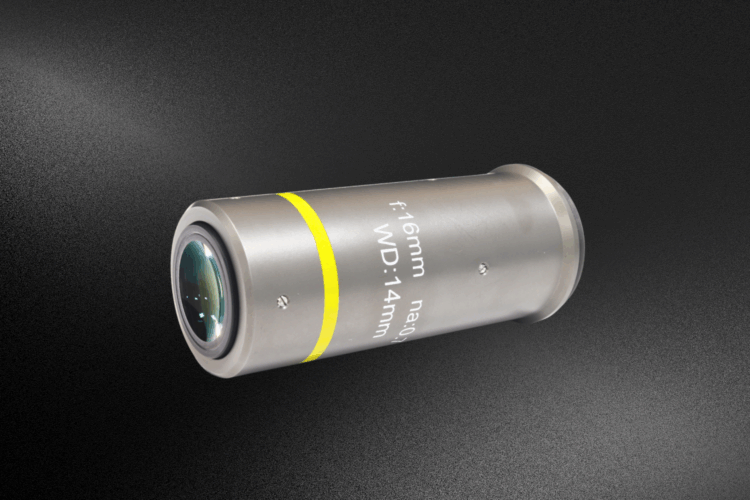
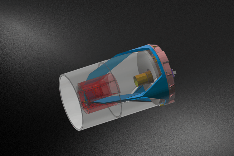
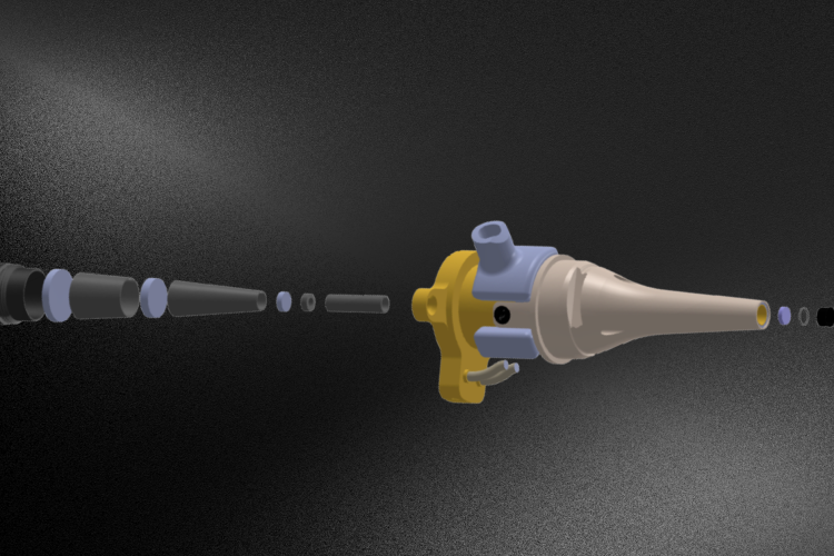
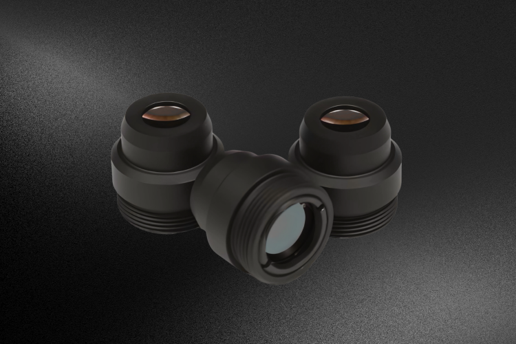
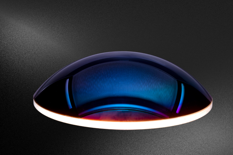
High NA and Long Working Distance Microscope Objective Lenses

Key Takeaways This case study examines the high NA infinity conjugate long working distance microscope objective, designed for optical tweezers and other precision applications. With a 16 mm focal length, 14 mm working distance, and 0.7 NA, this objective balances resolution and depth. Covering wavelengths from 420-900 nm, it supports various laser sources. The lens corrects for a 3 mm quartz window and requires precise machining due to high sensitivity to tolerances.  Performance testing ensures optimal imaging by adjusting eccentricity and air gaps. Overview of Optical Tweezers Technology  Optical tweezer technology is a tool that utilizes highly focused laser beams to capture and manipulate tiny particles, such as cells and nanoparticles. This technology generates force through the transfer of light, enabling non-contact control of small objects. The focused laser beam creates a strong gradient field near its focal point, attracting tiny particles to the region with high light intensity and thus facilitating capture.  Optical tweezers can manipulate nano-scale particles without causing physical damage to the samples and have demonstrated promising applications across various fields. To achieve effective particle capture in atom capture experiments, lasers typically need to converge to the micron level. Therefore, the microscope objective used in optical tweezer systems must possess high resolution. Increasing the numerical aperture (NA) is one useful method for obtaining high-resolution objective lenses. Since the samples for atom capture experiments are often placed in a vacuum chamber, the microscope objective must also provide a long working distance.  In recent years, microscope objective developers have focused on achieving both high NA and long working distances. High NA microscope objectives are extensively employed in fields such as biology, materials science, and semiconductor detection due to their high resolution and light-gathering ability. Generally, microscope objectives with high NA have shorter working distances. Achieving both high NA and long working distances necessitates the correction of numerous higher-level aberrations during the design phase, leading to complex structures, larger sizes, increased sensitivity to tolerances, and significant design and production challenges. Description of the High NA Objective This specific high NA microscope objective features a numerical aperture of 0.7 and a working distance of 14 mm, resulting in a larger diameter than conventional objectives. Its wide working band, which covers wavelengths from 420 nm to 900 nm, makes it versatile for different laser sources. It is important to note that this objective is designed to correct a quartz window with a thickness of 3 mm; any deviation from this thickness during actual use may diminish the performance of the objective. Working distance is the distance between the observed or processed object and the front end of the lens.  In practical applications, taking into account working distance is crucial when selecting a microscope objective. Typically, a longer working distance offers greater flexibility in application. However, for a fixed NA, increasing the working distance necessitates a larger lens size, while also increasing advanced aberrations within the optical path and complicating the manufacturing process. Additionally, a smaller ratio of focal length to working distance can result in increased spherical error from the rear lens due to the expansion of the optical path aperture, further complicating design efforts. Taking all this into account, the lens is designed with a focal length closely matching the working distance, which is 16 mm, and exhibits low magnification. Specification of the NA0.7 infinitely conjugated long working distance microscope objective Focal length 16mm NA 0.7 Wavelength 420-900nm FOV Φ0.5mm Working distance 14mm(including 3mm fused silica) NA0.7 Infinite conjugate long working distance microscope objective design structure Spot and WFE performance Performance Criteria of the Microscope Objective  The performance of the microscope objective is evaluated based on the size of the dispersion spot and the trans-wavefront error. The design value for the spot radius along the optical axis of this lens is less than 0.4 µm, indicating effective spot convergence at the micron level. Analysis of the transmit-wavefront diagram shows that this objective achieves diffraction-limited performance across various wavelengths, although the off-axis performance slightly exceeds the diffraction limit at 421 nm. Focal shift curve Chromatic Aberration and Wavelength Range  One unique feature of this lens is its operation across a wide range of wavelengths, from violet to near-infrared. Although the correction of chromatic aberration does not meet the diffraction limit, this objective lens has been specifically designed to perform well with laser sources. Only minimal post-focusing adjustments are required when using different light sources, helping to mitigate performance degradation caused by chromatic aberration. For the 421 nm band, the transmission wavefront design performance after focusing is as follows. transmission wavefront error@421nm Design Summary of High NA and Long Working Distance Microscope Objective Lenses The magnification of this micro objective lens is low, approximately 12X when paired with a 200 mm tube lens. The numerical aperture is significant, reaching 0.7, and the working distance extends to 14 mm, with correction for a 3 mm thick quartz window. The objective operates across a broad range of wavelengths from 421 to 900 nm, is compatible with various laser sources, and represents a special type of high-end objective. Optical Component Machining  Given the specific parameters of this objective lens, the effect of tolerance is highly sensitive, requiring precise machining tolerance for all components. The high NA and long working distance further heighten the challenges associated with manufacturing such optical components.  A frame for adjusting this micro objective lens Objective Focusing and Performance Testing  When adjusting the micro objective lens, it is essential to obtain an image of the object and adjust the lens’s eccentricity and air gap based on the imaging results. This process helps eliminate coma and spherical aberration that may arise from manufacturing deviations. The objective in question is a low-magnification microscope lens with a high numerical aperture (NA) and a large entrance pupil. When used with a standard microscope frame, the imaging results may be inadequate, making proper adjustment challenging. To ensure optimal performance, it is important to align the microscope with the object being observed. Measurement Graph: MTF vs. Frequency Customize

Read more
Case Study – UV Microscope Objectives for Genetic Analysis

Key Takeaways A global leader in agricultural genetics sought durable, cost-effective UV microscope objectives.  Challenges included optical design complexity, wavefront control, and fabrication precision.  By optimizing coatings, manufacturing, and materials, we extended the lens lifespan from 3 to 18 months, reducing replacement costs and downtime.  Avantier’s customized optical coatings improved both performance and durability, ensuring reliable genetic analysis. This collaboration set a new standard for high-performance, cost-efficient UV microscope objectives in genetics and reproduction. Project Background:  UV Microscope Objectives for Genetic Analysis A global leader in agricultural genetics and reproduction services approached us to address problems they were facing related to the cost and durability of microscope objective lenses. These lenses play a pivotal role in analyzing genetic data, directly impacting the company’s efficiency and operational costs. By partnering with us, they hoped to enhance the performance and longevity of their UV microscope objectives. Challenges in Designing and Manufacturing UV Microscope Objectives Optical Design Complexity Designing UV microscope objectives involves navigating the unique properties of UV light, such as shorter wavelengths, higher photon energy, and lower transmittance. Advanced optical design techniques needed to be employed to deliver optimal imaging across the entire field of view. One aspect of this was the development of apochromatic equation systems to correct chromatic and spherical aberrations. Material Selection and Manufacturing Processes UV-grade fused silica, prized for its high damage threshold and minimal scattering properties, was selected as the primary substrate. A specialized process was implemented during manufacturing to ensure the highest levels of cleanliness and mitigate potential contamination that could compromise imaging quality. Wavefront Aberration Control Maintaining wavefront aberration below λ/5 across the full wavelength range was crucial for achieving high-resolution, low-distortion imaging. This required meticulous optimization in both the design and manufacturing stages. Precision Fabrication and Testing The high photon energy associated with UV light demands exceptional surface quality and precision in optical components. Advanced fabrication techniques, coupled with state-of-the-art metrology technologies, were employed to meet these exacting requirements. Cost and Efficiency Challenges High production costs traditionally limit the widespread adoption of UV microscope objectives. Addressing this, we focused on reducing manufacturing expenses while maintaining stringent quality standards and optimizing production efficiency. Solutions and Outcomes Customized Optical Coatings To meet the company’s specific needs, a customized optical coating solution was developed in collaboration with Avantier. These coatings enhanced the durability and performance of the microscope objectives, enabling them to withstand the demanding conditions under which they were used.  Significant Longevity Improvements Through the implementation of advanced materials, coatings, and precision manufacturing processes, the operational lifespan of the UV microscope objectives was extended from 3 months to 18 months—a sixfold increase in durability.  Cost and Time Savings The extended longevity of the lenses drastically reduced the frequency of replacements, leading to substantial cost savings and minimized instrument downtime. This improvement streamlined the operations of the genetic analysis company, enabling them to allocate resources more effectively. UV Microscope Objectives for Genetic Analysis Enhancing UV Microscope Objectives  By addressing the complexities of UV light, selecting the best materials, and employing cutting-edge manufacturing techniques, we successfully delivered a robust solution that exceeded our client’s expectations. The collaboration not only resolved their immediate challenges but also set a new benchmark for cost-efficient, high-performance UV microscope objectives in the field of genetics and reproduction. Please contact us if you’d like to request a quote on your next project. Related Content

Read more
OAP Mirrors: Applications Across Industries
Off-axis parabolic mirrors applications

OAP Mirrors: Applications Across Industries Off-axis parabolic (OAP) mirrors are indispensable components in modern optical systems, offering precision and versatility in a variety of applications. These mirrors enhance performance by eliminating central obstructions and reducing aberrations. Their applications range from astronomy to laser systems. Here, we highlight three case studies that showcase the capabilities of OAP mirrors in different industries.   1. Terahertz and Infrared Applications In terahertz and infrared applications, precise optical paths are critical for accurate data acquisition and system performance. OAP mirrors are integral to constructing these paths, ensuring minimal wavefront distortion and high reflectivity. Specifications: Mirror Type: Large aperture off-axis parabolic mirror Aperture: 300mm Surface Accuracy: <1/3λ Coating: Dielectric film Off-axis Angle: 40° Material: Zerodur Large aperture off-axis parabolic mirror 2 In one notable implementation, a 300mm aperture OAP mirror with a dielectric coating was used to guide terahertz waves in a high-precision spectroscopy system. Its surface accuracy of <1/3λ and stable Zerodur material ensured reliable performance, even under temperature fluctuations, making it a cornerstone for cutting-edge research. 2. Astronomical Telescopes For astronomers, achieving unobstructed views of celestial bodies is paramount. OAP mirrors in telescopes minimize optical interference, enabling clear and detailed observations. Specifications: Mirror Type: Large aperture off-axis parabolic mirror Aperture: 400mm Surface Accuracy: <1/2λ Coating: Protected silver (Ag) Off-axis Angle: 30° Material: Fused silica Large aperture off-axis parabolic Mirror 1 A 400mm aperture OAP mirror with a protected Ag coating has been instrumental in enhancing the performance of a next-generation astronomical telescope. Its high surface accuracy and off-axis design reduced stray light and diffraction, providing sharper images of distant stars and galaxies. 3. Laser Systems Precision in laser beam control is essential for applications such as processing, communication, and research. OAP mirrors enable accurate focusing and path alignment, significantly improving system efficiency. Specifications: Mirror Type: Conventional off-axis parabolic mirror Apertures: 1 inch and 1/2 inch Surface Accuracy: <1/4λ Coating: Protected Ag or Au Off-axis Angle: 45° Material: 6061 Aluminum Conventional off-axis parabolic mirror In a laser system designed for industrial material processing, a conventional OAP mirror with a 1-inch aperture and protected gold (Au) coating was used to focus high-intensity beams. The 45° off-axis angle and high reflectivity ensured minimal energy loss, while the robust aluminum construction offered durability in demanding environments. The Versatility of OAP Mirrors These case studies underscore the adaptability of OAP mirrors in diverse fields. Whether enabling precise terahertz spectroscopy, enhancing celestial observations, or optimizing laser systems, OAP mirrors are critical to advancing optical technology. By tailoring specifications such as aperture size, coating, and material, manufacturers meet the unique demands of each application, pushing the boundaries of what is possible. Custom Off-Axis Parabolic Mirrors At Avantier Inc., we specialize in creating custom high-performance Off-Axis Parabolic (OAP) Mirrors designed for a wide range of applications. Our coating options include protected gold, silver, and aluminum, with protected aluminum being a preferred choice for visible and infrared applications. We offer SM-threaded, unthreaded, or post-mountable adapters for any of our in-stock OAP mirrors. To explore our stock options, visit our Stock – Off-Axis Parabolic Mirrors page. Our OAP mirrors are precision diamond-turned to ensure a smooth surface with minimal roughness. For a custom optical mirror tailored to your specific focal length and requirements, contact us today via our contact page. Related Content

Read more
Silicon Carbide Mirror for Aerospace Applications

Key Takeaways The Silicon Carbide Mirror for Aerospace combines a lightweight design, thermal stability, and high reflectance for optimal performance in extreme conditions. With precise dimensions (±0.1 mm) and exceptional surface accuracy (RMSI < 16 nm), it delivers clear, distortion-free imaging for satellite and deep-space applications. Its durable protective coating (>95% reflectance) withstands harsh environments. Proven in a space mission, the mirror enhanced imaging accuracy, reduced mission weight by 15%, and demonstrated exceptional reliability over two years of operation. Project Overview The Silicon Carbide Mirror was specifically designed to meet the stringent requirements of aerospace engineering, ensuring exceptional performance in challenging conditions. Its lightweight structure, combined with superior optical properties, makes it a critical component in space exploration and satellite imaging systems. Satellite imaging systems Key Challenges Addressed Thermal Stability: Aerospace environments demand materials with low thermal expansion. Silicon carbide’s excellent thermal conductivity and minimal expansion make it ideal for high-temperature and vacuum conditions. Precision Optics: The tight dimensional tolerance (±0.1 mm) and outstanding surface accuracy (RMSI < 16 nm) ensure optimal imaging performance, even for demanding space missions. Durability in Harsh Environments: The protective silver coating provides high reflectivity (>95%) across a broad wavelength range (400-12,000 nm), while also shielding the mirror from corrosion and mechanical damage in extreme conditions. Innovative Design Features Compact Dimensions: At 379 mm x 260 mm x 85 mm, the mirror balances size and performance, making it suitable for tight payload constraints. High Reflectance Coating: The mirror’s coating optimizes performance for wavelengths critical in infrared and visible spectroscopy used in aerospace applications. Advanced Material Composition: Silicon carbide combines lightweight characteristics with robust mechanical strength, enhancing reliability during launch and operation in orbit. Silicon Carbide Mirror for Space Application Product Specifications Material Silicon Carbide Dimensions Length: 379 mm, Width: 260 mm, Thickness: 85 mm Dimension Tolerance ±0.1 mm Clear Aperture 90% Surface Quality 80-50 Surface Accuracy  RMSI < 16 nm Coating Protective Ag Reflectance (Rabs) >95% @ 400-12,000 nm Angle of Incidence (AOI) 0 – 4.5° Application Highlights Satellite Imaging: The mirror’s high surface quality (80-50) and accuracy ensure clear, distortion-free images essential for earth observation and mapping. Astronomical Observations: Its precision and high reflectivity are key for capturing faint celestial objects in deep-space telescopes. Lidar and Laser Systems: The mirror’s consistent performance at various angles of incidence (0-4.5°) makes it valuable for space-based Lidar systems. Performance Metrics A recent deployment in a space mission demonstrated the mirror’s capabilities: Achieved clear imagery with minimal distortion during a temperature fluctuation range of -50°C to +60°C. Maintained reflectance above 95% over a two-year observation period. Successfully integrated into the payload, reducing overall mission weight by 15% compared to conventional mirrors. Customer Impact By utilizing the Silicon Carbide Mirror, the aerospace client has achieved: Enhanced imaging accuracy, contributing to critical data collection for climate research. Cost-efficiency in mission planning due to the material’s longevity and reduced maintenance needs. Related Content

Read more
Electromagnetic Shielding Grids in Optical Machining

Key Takeaways Electromagnetic shielding grids (ESGs) in optical machining are essential for shielding sensitive equipment from electromagnetic interference (EMI).  Customizable in aspects like shape, aspect ratio, and line width, these metal grids enhance shielding efficiency while maintaining high transmittance for optical needs. ESGs ensure signal integrity, measurement accuracy, and surface quality in high-precision settings.  Widely used across aerospace, defense, and high-tech industries, ESGs enable precision machining in interference-free environments, adhering to strict electromagnetic compatibility (EMC) standards. Electromagnetic Shielding Grids in Optical Machining With rapid advances in electronics and wireless technology, electromagnetic interference (EMI) has become a major concern, often impacting the performance of sensitive equipment. ESGs have therefore become crucial, especially in optical machining, where electromagnetic stability is key. These fine metal meshes act as barriers against electromagnetic waves, creating a controlled environment that allows for high-accuracy operations. Here’s a closer look at how ESGs work, their core parameters, different types, and the roles they play in optical machining. What is an Electromagnetic Shielding Grid? An electromagnetic shielding grid is a metal mesh structure designed to reduce or block electromagnetic waves,  EMI from affecting nearby devices. ESGs work by reflecting or absorbing the electromagnetic waves, creating a buffer zone around sensitive electronic or optical equipment. In optical machining—where accuracy is paramount—their use minimizes interference that could skew measurements, affect equipment stability, or impact machining quality. Grid Shape: ESGs are available in circular, random, or hexagonal configurations, with each shape offering unique shielding and transmission benefits. Circular grids, for example, may enhance transmission uniformity, while random grids suppress resonance at particular frequencies. Aspect Ratio: This is the ratio between the conductive material’s width and the grid’s total width. Higher aspect ratios boost shielding but may reduce transmittance, which is essential to balance in applications requiring both high shielding and optical clarity. Line Width and Width Ratio: In some ESGs, the width and spacing of grid lines are distributed randomly, which minimizes resonance with specific frequencies. Typically, line widths range from 0.1 mm to 1 mm, adjusted to accommodate specific application needs and frequency requirements. This versatility allows for tailoring the ESG to block out different interference frequencies effectively. Grid Spacing and Period: The spacing between grid lines significantly affects shielding at higher frequencies, with small grids commonly used in GHz applications for military and industrial purposes. Contact Resistance: Lower contact resistance (ideally below 1 milliohm) enhances the grid’s shielding performance by ensuring effective current transfer. Shielding Efficiency: Shielding efficiency measures the grid’s ability to block electromagnetic waves, typically expressed in decibels (dB). Higher efficiency (e.g., -60 dB to -100 dB) is necessary in military or high-tech industrial settings, where EMI could jeopardize sensitive operations. For example, an efficiency of -80 dB in a 1MHz to 1GHz range can significantly reduce interference, creating a controlled environment essential in optical machining. Transmittance: In optical applications, ESGs must often balance transparency and shielding. Optical transmission grids can achieve transmittance as high as 80-90% for visible applications. For infrared or other wavelength-specific uses, transmittance can be adapted between 50% and 85%, ensuring that the shielding properties do not impede optical performance. Types of Electromagnetic Shielding Grids Different grid types are chosen based on specific requirements: Metallic Grids: Made from copper, tin, or stainless steel, they provide excellent conductivity and durability, common in aerospace and petrochemical applications. Ferromagnetic Grids: Built from materials like permalloy, these grids are effective for shielding low-frequency magnetic fields. Composite Grids: Combining materials such as copper and permalloy, they offer broad shielding across multiple frequency ranges. Advanced Materials (e.g., Graphene Grids): Graphene’s lightweight, transparent, and low-reflective properties make it ideal for high-tech applications that demand both shielding and optical clarity. Applications of Electromagnetic Shielding Grids in Optical Machining ESGs play a vital role in maintaining precision and stability in optical machining: Protecting Sensitive Components: High-precision optical machining equipment integrates sensitive electronic components, including sensors, controllers, and lasers. These parts are highly susceptible to EMI, which can disrupt performance or even damage delicate circuitry. ESGs shield these components, ensuring accuracy and durability over prolonged use. Improving Measurement Accuracy: Measurement accuracy is essential in optical machining, where even minor inaccuracies can lead to substantial defects. EMI can impact instruments like lasers and beam modulators, causing data deviations. ESGs help maintain measurement precision by reducing EMI, resulting in consistently accurate data. Ensuring Signal Integrity: During optical machining, signal integrity is vital for transmitting accurate data. ESGs placed strategically within the equipment prevent EMI from distorting signal clarity, which directly impacts machining precision and effectiveness. Maintaining Surface Quality of Workpieces: In certain processes, EMI can introduce vibrations or temperature fluctuations that affect the workpiece’s surface finish. By stabilizing the environment, ESGs reduce the chances of surface imperfections, leading to higher-quality machining outcomes. Meeting Electromagnetic Compatibility (EMC) Standards: ESGs help ensure compliance with stringent EMC standards, aiding certification and market readiness. Circular grid Random grid Customization and Design Options The versatility of ESGs allows them to be customized to various shapes—such as random, circular, or hexagonal—suitable for curved surfaces, spherical windows, or other non-standard designs. Avantier’s ESGs are tailored to meet the exact needs of aerospace, defense, and precision machinery sectors, ensuring robust shielding without compromising flexibility. Conclusion Electromagnetic shielding grids have become integral in optical machining, providing EMI protection while preserving accuracy and quality. By selecting and customizing ESGs based on grid shape, line width, and shielding efficiency, Avantier enhances reliability, measurement accuracy, and surface quality. These advanced shielding solutions ensure that precision optical machining can occur in stable, interference-free environments, meeting industry standards and enabling the production of high-quality components. Related Content

Read more
Stress-Free Objective Lenses for High Precision Imaging

Key Takeaways Stress-free objective lenses offer superior imaging precision by eliminating internal stress, preventing distortion, and ensuring true image restoration.  Their design accounts for thermal expansion, reducing errors in varying environments.  Key applications include polarized light microscopy, scientific research, medical diagnostics, and industrial testing.  Advanced manufacturing processes, including precise material selection and assembly, ensure the stability and accuracy of these lenses.  Avantier’s custom stress-free objective lenses provide cutting-edge optical solutions, making them essential for high-precision fields. In the continuous evolution of optical technology, stress-free objective lenses have emerged as a leading solution, particularly for advanced polarized light microscopy. These lenses are designed to prevent signal distortion caused by stress during lens assembly, offering unique advantages for high-quality imaging. This article delves into the characteristics, principles, production processes, and applications of stress-free objective lenses, with a focus on their role in enhancing polarized microscopy. Features of a stress-free objective lenses The most notable feature of stress-free objective lenses is their excellent imaging stability and accuracy. By eliminating internal stress, these lenses effectively avoid imaging distortion and ensure accurate image restoration. Additionally, the design focuses on matching the thermal expansion coefficient of the materials, reducing imaging errors caused by temperature changes and enhancing the lens’s adaptability to various environments.  In advanced polarized light microscopy, stress-free objectives play a critical role in preventing distortion of polarized light interference signals caused by stress within the lens material. This stress, often introduced during lens assembly and curing, can interfere with the accuracy of detecting the crystallographic axis of crystal samples, as seen through a Boernet microscope. By using stress-free lenses, manufacturers ensure that optical performance remains stable, preserving measurement accuracy. While essential for high-end polarizing microscopes, stress-free optics limited applications in other areas where standard lenses suffice. The principle of stress-free objective lenses The design principle of stress-free objective lenses involves eliminating internal stress generated during manufacturing and assembly. This stress may arise from inhomogeneous lens materials, adhesive curing pressure, or mechanical assembly. By optimizing material selection, improving bonding processes, and using precision assembly equipment, stress-free lenses operate without external force influences, enabling accurate imaging in a stress-free state. The manufacturing process of the stress-free objective lenses The manufacturing process for stress-free objective lenses is complex and delicate. From material selection to processing, bonding, assembly, and inspection, every step must be strictly controlled. During lens bonding and assembly, advanced automated equipment and precise measuring tools are essential to maintain the lens’s stress-free state and imaging performance. Additionally, annealing is a key step in eliminating internal stress. Lenses material selection: When choosing lens materials, choose unstressed, birefringent materials. Lens structure: As shown in the figure below, the lens is fixed to the holder with the unstressed glue, and the holder should also be designed in the shape of a “worker”, so that when the holder is assembled, the extrusion stress on the holder will not be transmitted to the lens. Assembly without stress When the lens is assembled, the lens pressure ring and the pressure cap should be gently tightened, and then the low-stress glue to fix the pressure ring and the pressure cap on the mirror body. The following image is an example assembled as a normal microscope objective lens. Assembled Microscope Objective lens using stress-free objective lens Applications of stress-free objective lenses These lenses are widely used in fields requiring high-precision imaging, such as scientific research, medical treatment, and industrial testing. In scientific research, stress-free objective lenses provide scientists with accurate observation data. In the medical field, they enhance clarity for doctors observing internal structures, supporting diagnosis and treatment. In industrial testing, stress-free lenses are the preferred tool for detecting precision parts and materials due to their stability and accuracy. In conclusion, stress-free objective lenses play a vital role in modern optical technology, offering unique advantages. As science and technology continue to advance, and application demands increase, stress-free objective lenses will undoubtedly play an even greater role across various fields. Custom stress-free objective lenses by Avantier Our stress-free lenses represent a groundbreaking advancement in optical technology, offering unparalleled imaging precision and stability. Their innovative design and meticulous manufacturing process ensure the elimination of internal stress, making them a reliable choice for high-demand applications in research, medicine, and industrial testing. As the pursuit of superior imaging continues, stress-free objective lenses are set to lead the future of optical solutions. Ready to experience this innovation firsthand? Contact us today to learn more about how Avantier’s stress-free objective lens can elevate your optical systems. Related Content

Read more