
Solutions for the Performance Boundaries of Large-Aperture Spherical Lenses
Abstract
In the era of rapid advances in optoelectronic technology, large-aperture spherical lenses act as the “core pupil” of modern optical systems. Their performance determines the imaging precision and beam-control capability of high-end equipment—from deep-space telescopes to nanoscale lithography systems. Achieving nanoscale surface accuracy on millimeter-scale components represents one of the greatest challenges in optical manufacturing.
This application note introduces our advanced manufacturing technologies, precision testing systems, and real-world applications of large-aperture spherical lenses across multiple industries.
1. Core Technology: Achieving Harmony Between Size and Precision
The fabrication of large-aperture spherical lenses demands the perfect balance between millimeter-level dimensions and nanometer-level precision. The process encompasses three critical stages: material pretreatment, high-precision polishing, and performance verification. Through years of refinement, we have developed a reproducible, data-driven precision manufacturing system that ensures stability, consistency, and optical excellence.
1-1. Material Pretreatment: Ensuring Optical Uniformity and Stability
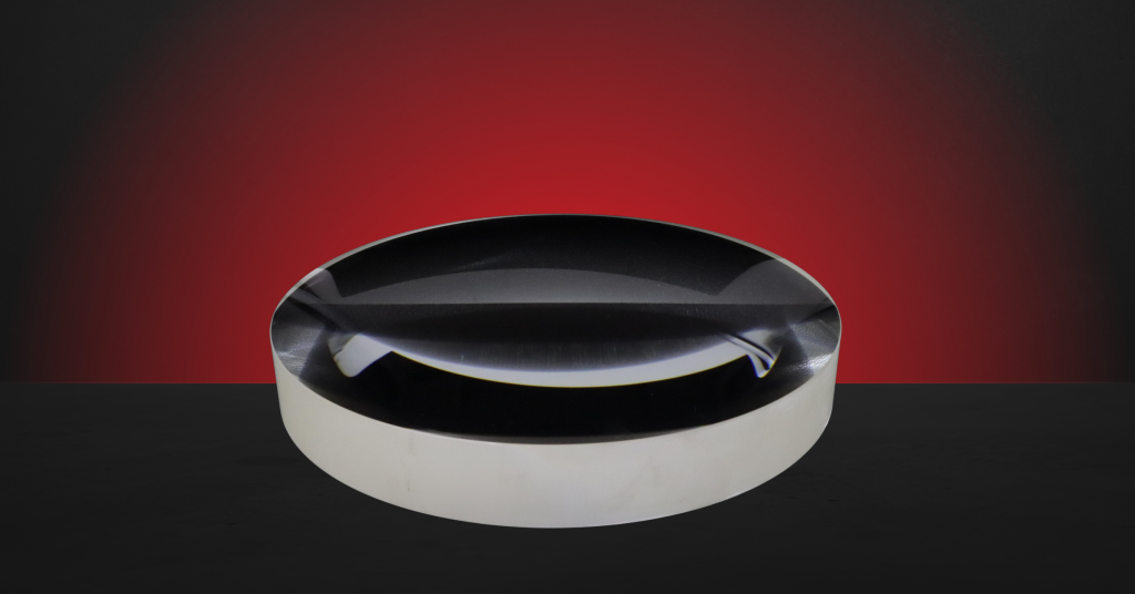
Selecting the right optical material involves balancing transmittance, thermal stability, and mechanical strength. Common materials include H-K9L optical glass, fused silica, and Zerodur® zero-expansion glass ceramics. Large diameters significantly increase handling and stress-control challenges.
For example, an 800 mm fused-silica lens can suffer surface warping if residual stress remains after cutting. To eliminate this risk, we employ a 72-hour slow-rate annealing process under precisely controlled temperature gradients. This process removes internal stresses and compositional inhomogeneities, ensuring long-term optical stability and uniform refractive index.
1-2. High-Precision Polishing: Integrating Surface Shape and Surface Quality
Polishing defines both the surface figure accuracy and surface roughness of a lens.
When a product must simultaneously meet specifications such as
- PV ≤ 1/3λ, RMS ≤ 1/200λ (λ = 632.8 nm), and
- surface roughness ≤ 0.2 nm with surface quality 10/5 (scratch-dig standard),
traditional methods like sandblasting and manual correction become insufficient.
To overcome these challenges, we integrate magnetorheological finishing (MRF) and ion beam polishing (IBP) into a unified, automated system.
Key Innovations
- Uniform Material Removal: A proprietary multi-axis dynamic pressure-compensation system minimizes magnetic-field attenuation at lens edges (up to 800 mm diameter), achieving uniform removal across the full aperture.
- Surface-Defect Control: Real-time optical feedback guides polishing to prevent micro-defects and “fog corrosion,” ensuring ultra-smooth surfaces of 0.2 nm roughness while maintaining ≥ 99.5 % transmittance in demanding lithography applications.
1-3. Precision Testing: Verifying Performance in Extreme Conditions
All lenses undergo comprehensive testing in an ultra-clean, vibration-isolated environment to guarantee accuracy and repeatability.- Large-Aperture Fizeau Interferometer: Enables full-aperture, no-blind-spot surface measurement for lenses up to 800 mm diameter.
- Constant Environment Control: Active vibration isolation (< 0.01 µm) and temperature stability (± 0.1 °C) ensure nanometer-level data reliability.
- Full-Area Defect Scanning: High-resolution light-scatterometry detects inclusions and bubbles as small as 10 µm, securing long-term product reliability.
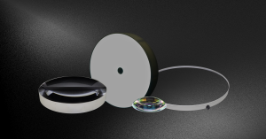
Large-Aperture Spherical Lens Manufacturing Capabilities by Avantier
Technical Index |
Specification / Range |
Diameter |
Φ10 mm – Φ800 mm |
Clear Aperture |
≥ 90 % |
Surface Accuracy |
PV ≤ 1/3λ, RMS ≤ 1/200λ (λ = 632.8 nm) |
Surface Quality |
60/40 – 10/5 |
Material Options |
H-K9L, N-BK7, Fused Silica, Zerodur, etc. |
Surface Roughness |
0.2 nm |
2. Product Applications: Powering High-End Optical Systems
Thanks to their exceptional precision and stability, our large-aperture spherical lenses are deployed across multiple advanced industries, enabling high-precision imaging, semiconductor fabrication, interferometric metrology, and industrial inspection.
2-1. High-Precision Imaging: Extending Vision from Medicine to Astronomy
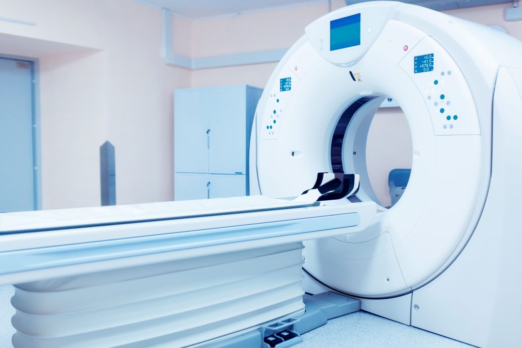
In medical imaging, large-aperture lenses form the optical core of high-end CT and MRI systems.
For instance, in a 320-slice CT scanner, a 150 mm spherical lens focuses X-rays onto a 500 mm-wide detector array. Our lenses achieve PV ≤ 1/5λ accuracy, ensuring clear image edges and reliable micro-lesion detection.
In astronomical research, our 1.1 m-class lenses deliver RMS ≤ 1/100λ stability, supporting long-exposure observation and deep-space imaging.
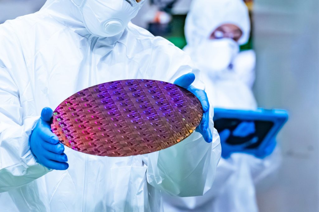
2-2. Semiconductor Lithography: Guaranteeing Nanometer-Scale Precision
Semiconductor lithography represents the highest-precision application for large-aperture spherical lenses.
In a 7 nm-class lithography system, multiple large lenses project design patterns onto wafers. Our 300 mm core lenses provide RMS ≤ 1/200λ (~ 3.16 nm) surface precision and ≤ 0.15 nm roughness, ensuring consistent wafer yield and minimizing pattern distortion.
2-3. Interferometry: The Foundation of Ultra-Precise Metrology
In high-precision interferometric measurement, spherical lenses generate standard reference wavefronts.
For example, a 200 mm lens used in aero-engine blade inspection focuses a laser into a 50 mm spherical wave, enabling contour deviation measurements with 0.1 µm accuracy.
For 300 mm semiconductor wafer flatness testing, a 400 mm lens achieves RMS ≤ 1/150λ, ensuring measurement errors under 0.05 µm—a critical parameter for photolithography alignment accuracy.
2-4. Industrial Inspection: The “Eye of Quality” in Automated Production
In automotive manufacturing, a 100 mm-diameter lens paired with a high-resolution camera enables single-shot imaging of entire engine-block surfaces, detecting micro-cracks as small as 0.1 mm without image vignetting.
In photovoltaic cell inspection, 250 mm lenses deliver 60/40 surface-quality imaging, identifying scratches and impurities on 182 mm and 210 mm wafers at speeds exceeding one wafer per second—ideal for high-volume production lines.
Advancing Large-Aperture Spherical Lens Precision and Performance
Large-aperture spherical lenses stand as the cornerstones of high-end optical engineering. Their fabrication pushes the limits of precision manufacturing, and their performance enables innovation across multiple industries.
Through rigorous process control, intelligent polishing systems, and strict metrology verification, we deliver not only components, but a commitment to precision, reliability, and continual excellence—providing the optical foundation for our clients’ most advanced projects.
🔎To learn more about our large-aperture spherical lens solutions or discuss custom optical manufacturing needs, please contact our engineering team.
Related Content

GREAT ARTICLE!
Share this article to gain insights from your connections!
