
Designs often converge near 114° not by convention but because physics, manufacturability, and practical constraints align there—balancing field of view, distortion control, and feasible optical complexity.

Designs often converge near 114° not by convention but because physics, manufacturability, and practical constraints align there—balancing field of view, distortion control, and feasible optical complexity.
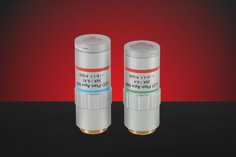
Near-infrared (NIR) microscopy objectives (780–2500nm) are essential for “seeing through” opaque barriers.
By balancing high resolution with superior penetration, they enable deep-tissue biological imaging, subsurface semiconductor defect detection, and non-destructive material analysis.
Despite design challenges like specialized material selection (ZnS/Germanium) and complex aberration correction, modern NIR optics provide high-transmittance solutions (≥ 85%) that surpass the physical limits of visible light, driving innovation in both high-tech manufacturing and life sciences.
Precision Telecompressors redefine imaging efficiency, pairing full-frame optics with smaller sensors while preserving field of view, sharpening detail, and strengthening low-light performance across advanced applications.
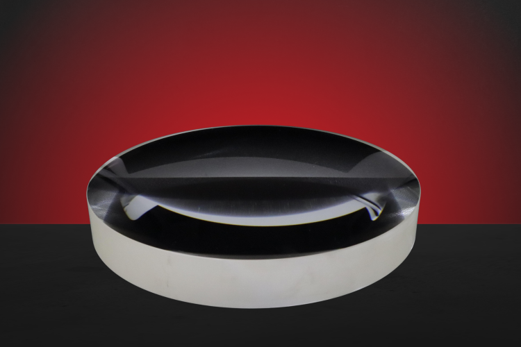
Large-aperture spherical lenses push optical manufacturing to extremes, combining nanometer-level precision with large-scale components to enable high-performance imaging, lithography, and precision metrology systems.

Lithography systems are essential to semiconductor manufacturing, enabling high-precision patterning through advanced exposure, alignment mechanisms, and specialized light sources to achieve high-resolution imaging.

With rapid advances in electronics and wireless technology, electromagnetic interference (EMI) has become a major concern, often impacting the performance of sensitive equipment.

Application of DLC film: Diamond-like hardness, corrosion resistance, and high transmittance make DLC ideal for enhancing infrared lenses.

The Germanium Optical Dome ensures optical clarity for drones by protecting optical instruments and maintaining their performance.

C-Lens manufacturing demands high-quality micro lenses with excellent surface quality and cost-effective production methods.

Aspheric lenses improve optical performance by reducing aberrations, delivering sharper images and better edge-to-edge clarity. They are thinner, lighter, and enable compact designs while maintaining high image quality.
