How Are Sub-Nanometer Precision Mirrors Manufactured?
Introduction: The Challenge of Manufacturing at the Atomic Scale
Producing optical mirrors with sub-nanometer precision is one of the most demanding tasks in modern manufacturing.
At this level:
Surface errors must be controlled to fractions of a nanometer
Even atomic-scale irregularities can affect performance
Conventional machining and polishing methods are no longer sufficient
To overcome these challenges, manufacturers rely on a fully integrated process chain that combines advanced materials, deterministic processing, precision coating, and real-time metrology.
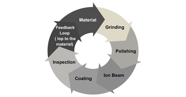
The Complete Manufacturing Workflow
The production of sub-nanometer precision mirrors follows a tightly controlled sequence:
Substrate material engineering
Ultra-precision machining and polishing
Optical coating
Closed-loop inspection and correction
Each stage is interdependent, and errors must be minimized and corrected continuously throughout the process.
End-to-end process flow for sub-nanometer precision mirror fabrication, where each stage is tightly controlled and continuously corrected through closed-loop feedback.
1. Substrate Material Engineering
The foundation of optical precision lies in the substrate.Common materials include:
Fused silica
Silicon carbide (SiC)
These materials are not used in their standard form. Instead, they undergo customized modification to enhance:
Thermal stability
Mechanical strength
Machinability
For high-end applications, thermal expansion coefficients can be reduced to extremely low levels (~5×10⁻⁸/°C), comparable to industry benchmarks such as ULE and Zerodur glass.In aerospace applications, modified SiC substrates offer:
Lower density
Higher specific stiffness
Improved thermal conductivity
This enables the production of lightweight yet stable large-aperture mirrors.
2. Ultra-Precision Machining and Polishing
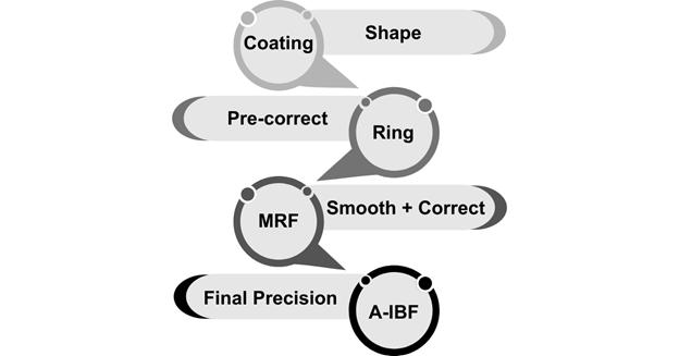
Achieving sub-nanometer surface accuracy requires a multi-stage process combining different techniques.
Ductile Grinding
↓
Ring Polishing
↓
MRF-CMP
↓
A-IBF
Multi-stage process for achieving sub-nanometer surface accuracy, integrating sequential deterministic and corrective manufacturing techniques.
2.1 Ductile Regime Grinding
The initial shaping stage uses ultra-precision grinding with cutting depths below 30 nm.This:
Minimizes subsurface damage
Establishes a high-quality starting surface
2.2 Ring Polishing
A preliminary polishing step rapidly improves surface form, bringing:
Surface profile error down to PV <50 nm
This prepares the mirror for fine correction processes.
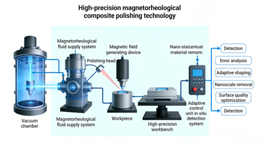
2.3 Magnetorheological Finishing + Chemical Mechanical Polishing (MRF-CMP)
One of the most critical technologies is the integration of:
Magnetorheological Finishing (MRF)
Chemical Mechanical Polishing (CMP)
MRF uses a magnetically controlled fluid to precisely remove material, while CMP enables ultra-smooth surface finishing.Together, they allow:
Rapid convergence of surface errors
Surface precision down to PV <5–10 nm
RMS values in the range of 0.5–0.8 nm
Real-time feedback systems adjust parameters such as:
Magnetic field strength
Rotation speed
Feed rate
This enables highly controlled and repeatable processing.
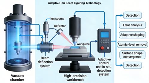
The final shaping stage is achieved through Adaptive Ion Beam Polishing (A-IBF).This technique:
Uses high-energy ions (e.g., Ar⁺)
Removes material at the atomic level
Operates without mechanical contact
Key advantages include:
Sub-nanometer surface correction
No induced stress or deformation
High precision in mid- to high-frequency error correction
Compared to traditional ion beam polishing, A-IBF introduces:
Real-time adaptive parameter tuning
Closed-loop control systems
Improved efficiency (over 30% increase)
This stage is essential for reaching final sub-nanometer accuracy.
Adaptive Ion Beam Figuring Technology
3. Optical Coating Technologies
After achieving the desired surface profile, mirrors require high-performance coatings.A key method is Ion Beam Sputtering (IBS), used to deposit multilayer dielectric films such as:
Ta₂O₅ / SiO₂
HfO₂ / SiO₂
These coatings provide:
Reflectivity up to 99.98%
High laser damage thresholds (35–40 J/cm²)
A major challenge in coating is stress control. Excess stress can deform the mirror surface.Advanced low-stress coating systems can:
Control stress within 30–50 MPa
Prevent post-coating distortion
Maintain long-term stability
4. Closed-Loop Metrology and Process Control
Precision manufacturing is only possible with equally precise measurement systems.Modern systems integrate:
Sub-nanometer in-situ metrology
Power Spectral Density (PSD) analysis
Digital twin simulation
These capabilities enable:
Detection accuracy of 0.03–0.08 nm (RMS)
Real-time error correction
Continuous process optimization
Closed-loop control ensures that:
Deviations are detected immediately
Processing parameters are adjusted dynamically
Final specifications are consistently achieved
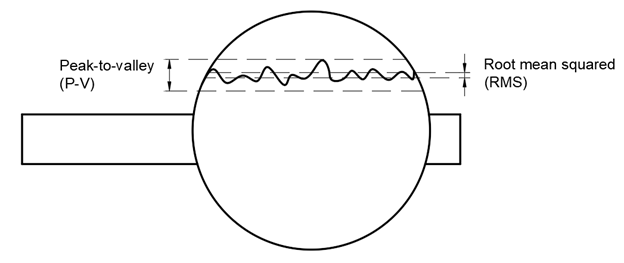
Understanding Key Performance Metrics
To evaluate mirror quality, several parameters are used:
RMS (Root Mean Square): measures overall surface error
PV (Peak-to-Valley): measures the maximum deviation
Ra (Average Roughness): indicates surface smoothness
Typical performance levels for sub-nanometer mirrors include:
RMS: 0.05–0.1 nm
PV: ≤ λ/100
Ra: 0.06–0.09 nm
These values represent world-leading precision in optical manufacturing.
Key surface metrology parameters used to evaluate mirror quality, including RMS, PV, and Ra, with typical performance levels achieved in sub-nanometer optical manufacturing.
Why Process Integration Matters
The key to achieving sub-nanometer precision is not a single technology, but system-level integration.Success depends on:
Coordinating multiple processes
Maintaining stability across stages
Enabling feedback between measurement and machining
This integration transforms manufacturing from a linear sequence into a closed-loop optimization system.
Conclusion: Engineering at the Limits of Precision
Manufacturing sub-nanometer precision mirrors requires a combination of:
Advanced material science
Deterministic machining techniques
Precision coating technologies
Real-time metrology and control
Together, these elements enable reliable, repeatable production at the limits of physical precision.As demand grows in fields such as semiconductor lithography, aerospace, and high-energy systems, these manufacturing technologies will continue to play a critical role in shaping the future of advanced engineering.