Lithography systems are vital for precise circuit patterning in semiconductor manufacturing.
Exposure methods like contact/proximity and projection are utilized to produce desired patterns.
Accurate alignment via global/local marks and interferometry is crucial, and the light sources used dictate resolution.
Extreme Ultraviolet Light (EUV) enables production of the finest features. Innovations in lithography are key to continued progress in shrinking semiconductor nodes and advancing the industry.
Lithography Systems Overview
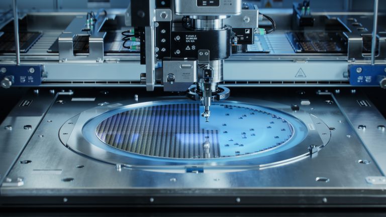
Lithography systems play a crucial role in semiconductor manufacturing, enabling the precise patterning of circuit features on silicon wafers. These systems utilize advanced exposure techniques, alignment mechanisms, and specialized light sources to achieve high-resolution imaging.
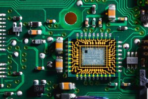
Lithography System in Semiconductor
Exposure Methods
Lithography systems employ various exposure techniques to transfer patterns onto wafers:
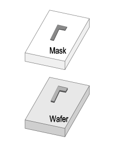
Contact and Proximity Lithography: These traditional methods involve direct exposure of the wafer to a mask, with proximity lithography providing a slight gap to minimize damage while maintaining reasonable resolution.
Projection Lithography: This method, utilized in modern semiconductor fabrication, employs optical systems to project an image of the mask onto the wafer at a reduced scale and with enhanced resolution and throughput.
Projection Lithography Schematic Image
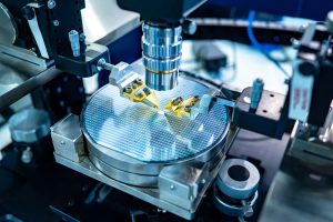
Alignment and Positioning
Accurate alignment is essential for ensuring precise pattern overlay on wafers. Lithography systems incorporate advanced alignment mechanisms such as:
Global and Local Alignment Marks: These reference points help in precise layer-to-layer alignment.
Interferometric Positioning Systems: In high-end lithography tools, these systems provide nanometer-level accuracy in wafer positioning.
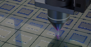
Light Sources and Optics
The choice of light source significantly impacts lithographic resolution and pattern fidelity. Popular options include:
Mercury Lamps and Deep UV (DUV) Lasers: Traditional sources for lithography, these lamps and lasers are primarily utilized for older nodes.
Excimer Lasers (KrF, ArF): These ultraviolet lasers are widely used in modern semiconductor fabrication due to their ability to achieve fine feature sizes.
Extreme Ultraviolet (EUV) Sources: The latest advancement in lithography, EUV light at 13.5 nm enables patterning of the smallest feature sizes in advanced semiconductor nodes.
Conclusion
Lithography systems are essential to semiconductor manufacturing, enabling high-precision patterning through advanced exposure, alignment, and optical technologies. As semiconductor nodes continue to shrink, innovations in lithography will remain critical to the industry’s progress.
Avantier is a trusted partner in semiconductor optics, offering high-precision microlens array solutions tailored to the demanding requirements of the industry. Our advanced lithography capabilities and state-of-the-art equipment enable the fabrication of custom microlens arrays with exceptional accuracy and consistency. Our team has deep expertise in optical modeling and material selection, and they collaborate closely with clients to deliver performance-optimized designs. Contact us today to explore how our semiconductor optics solutions can support your next innovation.