
Key Takeaways
- Semiconductor manufacturing requires high-precision optical lens assemblies. Custom objectives face challenges like miniaturization, thermal instability, and cost.
- Semiconductor lens assembly solutions include advanced fabrication, adaptive optics, and thermally stable materials.
- Key design considerations are optical performance (NA, chromatic correction, FOV), material selection (low dispersion, high transmittance), and specialized coatings.
- Meeting these demands requires a collaborative approach and cutting-edge manufacturing to ensure reliable performance in harsh fab environments.
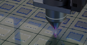
In today’s rapidly advancing technological landscape, semiconductor manufacturing pushes the boundaries of precision and miniaturization. Custom objectives, essential optical components within sophisticated imaging systems, are at the heart of this progress, enabling. These intricate optical lens assemblies enable critical processes like photolithography, wafer inspection, and metrology.
This summary delves into optical design considerations for these custom optical systems, exploring the challenges and highlighting innovative assembly solutions. From high NA microscope objectives to complex multi-element lenses, achieving optimal system performance requires careful attention to optical performance, material selection, coating requirements, and robust manufacturing capabilities.
Design Considerations for Custom Objectives:
When designing custom objectives for semiconductor manufacturing and inspection, there are three areas that need special attention: optical performance, materials selection, and coating requirements.
- Optical Performance
Key parameters include:
- Numerical Aperture (NA): High NA (often >0.95) is essential for sub-wavelength resolution.
- Chromatic Correction: Objectives must perform consistently across multiple wavelengths (e.g., DUV, EUV).
- Field of View (FOV): Balancing high resolution with a wide FOV is crucial for throughput. Aspheric or freeform lenses may be required.
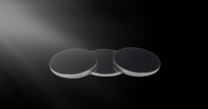
- Material Selection:
Materials must exhibit:
- Low Dispersion: Minimizes chromatic aberration.
- High Transmittance: Maximizes light throughput, especially in UV/DUV.
- Environmental Stability: Resistance to temperature variations, chemicals, and radiation. Examples include fused silica and CaF2.
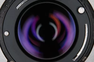
- Coating Requirements:
Essential coatings include:
- Anti-Reflection (AR): Minimizes light loss and enhances contrast.
- Hard Coatings: Protect lens surfaces from damage.
- Bandpass Filters: Isolate specific wavelengths for metrology and inspection.
Challenges and Solutions:
Miniaturization, thermal stability, cost, and environmental challenges can complicate the design process and require carefully crafted solutions.
Miniaturization and Complexity: Smaller devices require increasingly complex lens assembly designs and tighter tolerances.
- Challenge: Achieving nanometer-level accuracy in lens alignment and managing higher-order aberrations in high-NA systems.
- Solution: Adaptive optics, freeform lens technologies, and advanced fabrication techniques (e.g., diamond turning, computer-controlled polishing).
Thermal Stability: Semiconductor environments experience thermal fluctuations that can degrade lens performance.
- Challenge: Maintaining optical performance despite temperature variations.
- Solution: Thermally stable materials (e.g., fused silica, ULE glass), athermal designs, and active cooling systems.
Cost Considerations: Developing high-end custom objectives is expensive, especially for low-volume production.
- Challenge: Balancing performance with cost effective solutions.
- Solution: Collaborative development with optical suppliers, standardized modular designs, and rapid prototyping.
Environmental Challenges: Semiconductor fabs present harsh environments with contaminants, vibrations, and chemicals.
- Challenge: Protecting lenses from these factors.
- Solution: Protective coatings, vibration isolation systems, and purge systems can maintain a clean optical path.
The Future of Semiconductor Lens Assembly Solutions
Designing custom objectives for semiconductor applications demands a multifaceted approach, taking into account the complex interplay of optical, material, and environmental factors. Continuous innovation in design, fabrication, and environmental control is necessary in order to meet the stringent quality standards and performance requirements of this industry. Addressing the challenges posed by miniaturization, thermal instability, cost constraints, and harsh environments requires a collaborative effort, leveraging the expertise of a skilled engineering team with advanced manufacturing capabilities.
Optical advances such as active alignment techniques and a wider range of optical lens assembly types are crucial for ensuring the reliable performance of optical systems in semiconductor manufacturing. Avantier, an ISO 9001 certified company, offers high NA microscope objectives and customized solutions with cutting-edge technologies, manufactured and tested to the highest quality standards. Contact us today for your next project in semiconductors or any other industry that requires high-performance optical systems.


GREAT ARTICLE!
Share this article to gain insights from your connections!