Avantier Microlens Arrays: Precision in Every Lens
Avantier specializes in the design and manufacturing of high-performance microlens arrays (MLAs)—compact optical components engineered to deliver precise beam shaping, uniform illumination, and exceptional efficiency.
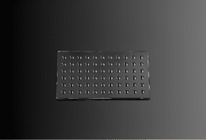
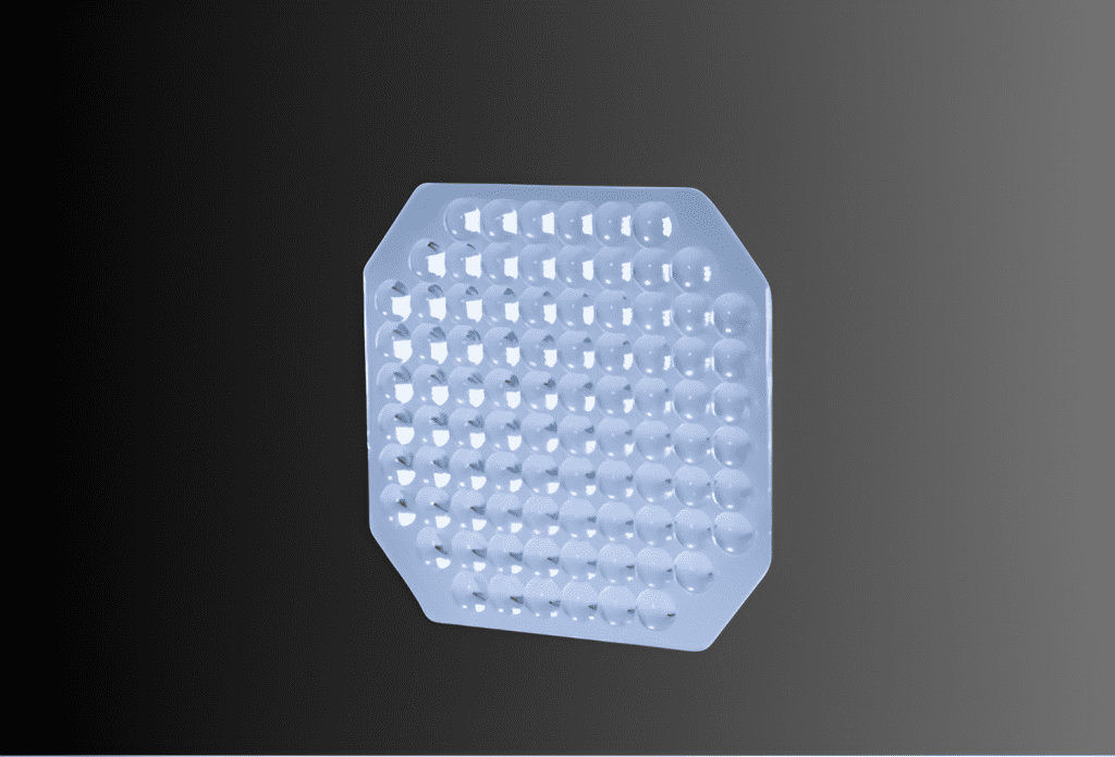
Microlens arrays, also known as microstructure lens arrays, consist of 1D or 2D grids of miniature lenses that collectively manipulate and homogenize light. They are indispensable in LiDAR, biomedical imaging, AR/VR systems, projection displays, and laser beam shaping, where reliability and accuracy are mission-critical.
Laser Systems: High efficiency beam homogenization and shaping
Aerospace & Defense: Rugged MLAs for mission-critical sensing and imaging
Wavefront Sensing & Astronomy: Shack–Hartmann arrays for adaptive optics and testing
Technical Advantages
Uniform Light Distribution: Eliminates hot spots and fluctuations
Compact Footprint: Ideal for miniaturized optical modules
High Transmission Efficiency: Reduced reflection and scattering losses
Customization Flexibility: Designed to match exact system requirements
Scalable Production: From prototypes to high-volume manufacturing
Technical Resource
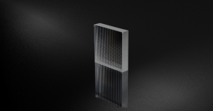
What is a Microlens Array?
A microlens array is a miniature optical device composed of thousands to millions of tiny lenses on a substrate, arranged in 1D or 2D grids. Each microlens functions independently yet contributes to collective light regulation, enabling beam homogenization, focusing, and advanced optical manipulation.
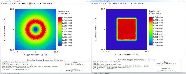
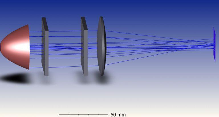
The diagram shows the light path, from left to right, consisting of the light source, reflector, lens array 1, lens array 2, collimator lens, and detector. There are a total of 2 detectors, one placed in front of lens array 1 and the other behind lens array 2.
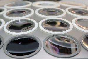
Lens Arrangements
Rectangular Grid: Ideal for alignment with pixel arrays
Hexagonal Close-Pack: Maximizes fill factor for circular lenses
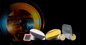
Avantier manufactures microlens arrays using several advanced technologies, including semiconductor lithography, laser micromachining, and precision glass molding.
Q: Are Avantier’s microlens arrays customizable? Yes. Every MLA is engineered to your system requirements—pitch, focal length, materials, coatings, and even array geometry.
Q: Which industries benefit most from MLAs? We support biomedical, automotive (LiDAR), AR/VR, aerospace, defense, and laser research markets worldwide.
Q: Do you offer prototyping before full production? Yes. We partner with clients through the entire process, from concept validation to volume manufacturing.
Partner with Avantier for Microlens Arrays
Avantier’s microlens arrays deliver world-class optical performance, tailored to the unique challenges of your application. Whether you require beam homogenization, precise light shaping, or compact imaging solutions, our engineering and production expertise ensures results that exceed expectations.
📩 Contact Avantier today to discuss your custom microlens array requirements and discover how we can accelerate your optical innovations.