
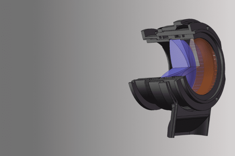
At Avantier, we are our proud of our track history in assisting customers to solve problems using reverse optical engineering. Here are three case studies.
At Avantier, we are our proud of our track history in assisting customers to solve problems using reverse optical engineering. Here are three case studies.
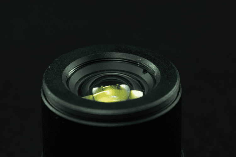
At Avantier we offer Design for Manufacturing (DFM services), optimizing product design with our extensive knowledge of manufacturing constraints, costs, and methods.