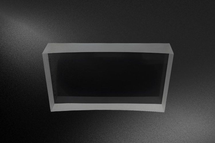
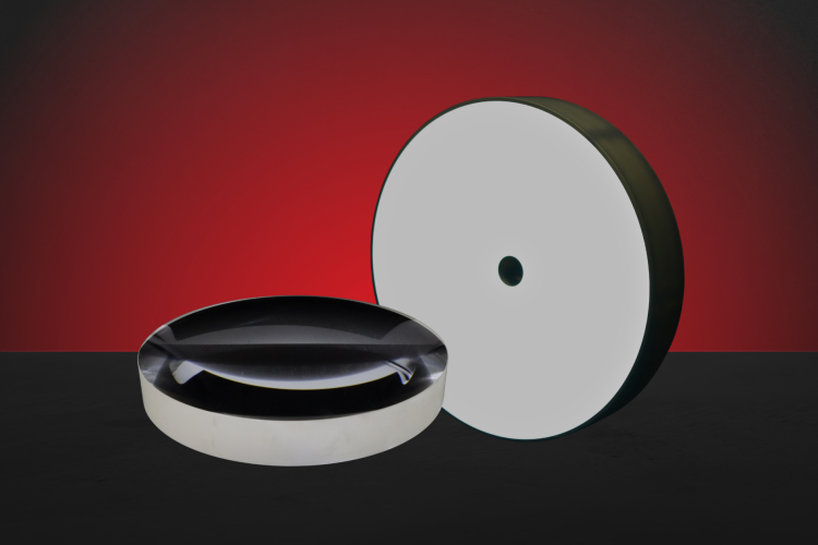
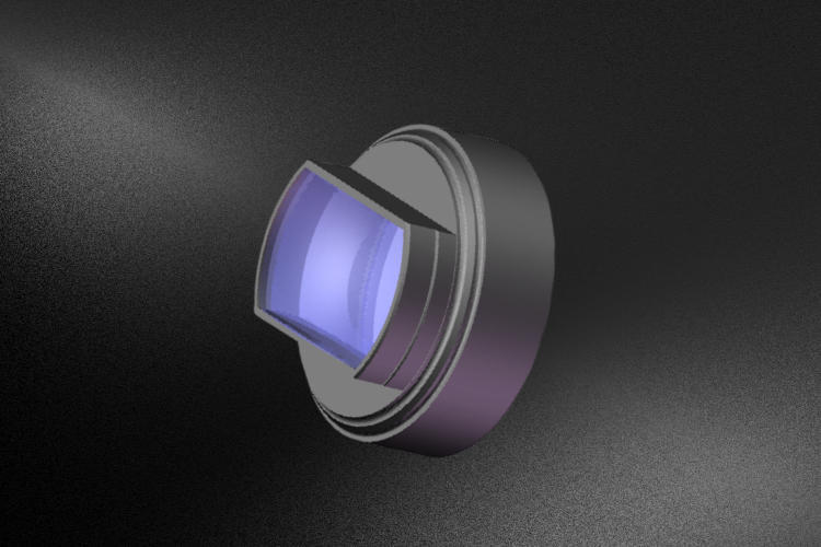
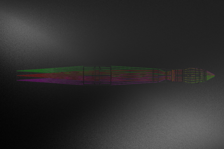
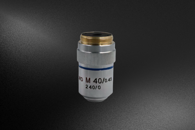
LiDAR VR/AR Applications: Powering Virtual Reality
LiDAR for AR/VR makes augmented or virtual reality more responsive, LiDAR VR AR, real time 3D

Key Takeaways LiDAR enables advanced VR experiences by providing precise, real time 3D spatial mapping.  Once bulky and expensive, modern LiDAR systems are now compact enough to fit into smartphones like the iPhone Pro 12.  This technology enhances VR/AR experiences with benefits such as better spatial tracking, faster virtual object placement, enhanced realism, and improved depth sensing.  Key specifications include detection range, range precision, accuracy, field of view, and scan patterns.  Avantier specializes in designing high precision LiDAR components, enabling customized solutions for AR/VR applications. LiDAR VR/AR Applications LiDAR VR/AR  applications are taking augmented and virtual reality applications to the next level. Once far to expensive and bulky for consumer applications, today a basic LiDAR system can be condensed to fit into a smart phone and cost less than a hundred dollars. Here we’ll look at just how they work, and what to expect from the combination of LiDAR and AR/VR. LiDAR for AR/VR makes augmented or virtual reality more responsive What is LiDAR? Think of LiDAR as optical radar. An acronym for Light Detection and Ranging, it uses light waves from a laser to create a highly accurate, super-speedy 3D map of an object or area. Wavelength of the laser is typically 250 nm to 11μm but depends on the application requirements. A quick working sensor makes time of flight  (TOF) calculations— determining just how long each laser pulse takes to reach the target and return— and uses this raw data  and point clouds to create a precise 3D map of terrain or objects and their placement in space. The intensity of the reflected light can provide extensive information, too, about the type of materials scanned and their density. LiDAR for AR/VR uses time of flight principles to determine the topology of an object or landscape LiDAR scanners were originally developed for research purposes, especially meteorology applications. It was successfully used to map the surface of the moon back in 1971, but the technology behind it has improved dramatically and LiDAR today is cheaper, faster, and more powerful than ever before. This new affordability is part of the reason behind the explosion of LiDAR use across real world industries today. We see it in self-driving cars, in speed enforcement, in stormwater management in agriculture— and in AR/VR. LiDAR and AR Before the integration of LiDAR with augmented reality, AR was limited by clunky machine vision systems that struggled to provide precise real time 3D mapping. Today, with precise spatial mapping at the speed of light, LiDAR gives AR and VR systems the potential to be faster, more accurate, and so more responsive. Today LiDAR for AR/VR can be condensed to fit inside a smartphone When Apple integrated a miniature LiDAR system into the 2020 iPad Pro and iPhone Pro 12, the power of LiDAR became available to AR and VR app makers for the first time. Since then, they’ve been experimented with extensively.  There’s more than one way that augmented reality (AR) and virtual reality systems can be improved by LiDAR integration. A few benefits of the integration include: Better Spatial Tracking Faster Placement of Virtual Objects Enhanced Realism Improved Depth Sensing LiDAR for AR/VR Specifications Producers of smartphones and AR and VR viewing devices today have the potential to take their viewer’s experience to the next level by incorporating LiDAR technology into their devices. But types and capabilities of LiDAR scanners vary greatly. Here’s a brief summary of some of the most important specs for AR/VR LiDAR. The LiDAR Detection Range gives the maximum distance at which LiDAR can detect an object. It is dependent on laser power, laser type, and aperture size.  While airborne LiDAR may be used to map surfaces hundreds to thousands of meters away, the types of LiDAR incorporated in consumer devices typically have a much more limited detection range. The iPhone Pro 12’s LiDAR, for instance, can scan at distances up to five meters.  LiDAR Range Precision tells you just how repeatable measurements will be. If precision is high, multiple measurements of the same object will cluster close to a mean value; but low precision tells you there is significant scatter. LiDAR Range Accuracy is like precision, but rather than comparing measurements to each other, it compares them to the actual distance. High accuracy means measurements are very close to the real distance. Field of View (FOV) refers to the angle over which the LiDAR system works: either the angle covered by the sensor or that which signals are emitted, whichever is smaller. A mechanically rotating system may have 360 degree field of view, but for many virtual reality applications, a smaller FOV is sufficient.  Scan Pattern tells you how the laser beam moves to perform its measurement, and includes information like point density and the number of scan lines. In some LiDAR scanners, this may be customizable. AR/VR LiDAR at Avantier Avantier is a premier producer of custom high precision optics, including LiDAR components and systems built to our customer’s exact specifications. Our expert engineers and designers are available to help you at any stage of the process, whether you’re doing your initial research or have a custom design ready to go.  Contact us today for your next project. References Applied Tech Review. LiDAR Powering Future AR/VR and Metaverse Experiences. May 2024.  Luetzenburg, G., Kroon, A. & Bjørk, A.A. Evaluation of the Apple iPhone 12 Pro LiDAR for an Application in Geosciences. Sci Rep 11, 22221 (2021).  Wandinger, Ulla. “Introduction to lidar.” Lidar: range-resolved optical remote sensing of the atmosphere. New York, NY: Springer New York, 2005. 1-18.  Related Content

Read more
OAP Mirrors: the complete guide
off-axis parabolic mirror, off-axis design, OAP coatings, OAP applications, chromatic aberration

Product Highlights Parabolic mirrors can focus collimated light without introducing spherical aberration. An Off-Axis Parabolic mirror  (OAP mirror) is a segment taken from a larger parabolic mirror.  When collimated light strikes an OAP mirror, it is focused to a point. Unlike a centered parabolic mirror, an OAP mirror offers the advantage of providing more space around the focal point, allowing for greater interaction with the beam without disrupting it. OAP mirrors offer precise beam control, are chromatic aberration-free, and come in various configurations.  Reflective coatings (metal or dielectric) enhance performance. The off-axis design and material choices impact cost and precision. Introduction to Off-Axis Parabolic Mirrors Off-axis parabolic mirrors (OAPs) are a widely used type of aspherical mirror, known for their ability to converge and collimate light beams efficiently. These mirrors are designed by extracting a portion of a parent paraboloid, resulting in unique optical properties. Unlike traditional lenses, off-axis parabolic mirrors leverage reflection, eliminating chromatic aberration and providing superior beam manipulation. Key Features and Advantages Precision Beam Control The paraboloidal surface of OAPs ensures perfect correction of spherical aberration, enabling precise convergence and collimation of light. The off-axis design separates the focus from the optical axis, allowing these mirrors to simultaneously perform beam steering while converging or collimating light. Chromatic Aberration-Free Unlike refracting optics, OAPs do not rely on material dispersion, making them ideal for applications requiring high optical precision across a broad spectrum of wavelengths. Core Parameters of Off-Axis Parabolic Mirrors Clear Aperture The clear aperture represents the maximum diameter of a parallel light beam that the mirror can handle. It is typically circular, ensuring efficient optical performance. Focal Length Focal length defines the distance between the mirror surface and its focal point: – Parent Focal Length: Distance from the paraboloid vertex to the focus, independent of the off-axis distance. – Effective Focal Length (EFL): Distance between the focus and the main reflected beam, influenced by the parent focal length and off-axis displacement. Off-Axis Distance and Angle The off-axis configuration is defined by: – Off-Axis Angle: The reflection angle of the main beam, typically between 0° and 90°. – Off-Axis Distance: The lateral distance between the paraboloid’s symmetry axis and the main ray. Customization Options OAP mirrors can be tailored with surface shape accuracy, reflectivity, surface finish, and additional features such as holes or mounting mechanisms based on user requirements. Diagram of an Off-axis parabolic mirror Reflective Coatings To maximize performance, OAP mirrors are coated with reflective films suited to specific applications. Below are the common coating types: Metal Coatings Aluminum Coating: Offers wideband reflectivity, particularly effective in the ultraviolet range when combined with magnesium fluoride. It is durable and economical, with reflectivity exceeding 80% in the visible spectrum. Silver Coating: Provides high reflectivity (95% in the visible and over 97% in the infrared) but is unsuitable for UV applications due to high absorption. Requires a controlled environment due to lower durability. Gold Coating: Optimal for infrared applications, with high reflectivity beyond 650 nm. Gold coated OAP mirrors are also highly resistant to laser damage and have minimal phase delay effects. Dielectric Coatings Dielectric coatings are multilayer stacks of materials with varying refractive indices. These coatings offer: – High Reflectivity: Can achieve over 99.9% reflectivity. – Custom Bandwidth: Tailored for specific wavelength ranges. – High Laser Damage Threshold: Suitable for high-power applications. Dielectric coatings are sensitive to incident angles, causing reflectivity peaks to shift towards shorter wavelengths at higher angles. OAP Mirror Applications Off-axis parabolic mirrors are indispensable in fields such as: Astronomy Laser systems Spectroscopy Optical communications Biomedical imaging Their unparalleled optical precision and versatility make them essential components in advanced optical systems. By understanding their core parameters and coating options, users can effectively integrate OAPs into their applications for optimal performance. Design specifications OAP mirrors have a complex design that requires careful attention to detail and advanced knowledge for successful creation. Only skilled engineers can design a specific OAP mirror that meets the necessary specifications and is suitable for its intended application. This section includes a schematic of the OAP mirror.  Detailed image of OAP Mirror The beam’s aperture can be either circular or square and is aligned with the Z axis. Depending on the angle, the size of the aperture on the optical surface may look elliptical or rectangular. For optics with large off-axis angles or apertures, a non-wedge design is often more affordable. This design allows you to set a tilt angle in relation to the main Z axis. You can make off-axis parabolic mirrors (OAP mirrors) from different materials, like metals (using single-point diamond turning), glass, and special ceramics such as SiC. The material you choose will greatly affect both the cost and precision of the mirrors. For more information, please visit the in-depth article. ” OAP Mirror “ Examples of projects The following is a physical introduction of the off-axis parabolic mirror: Conventional off-axis parabolic mirror Aperture: 1 inch and 1/2 inch, Surface accuracy: <1/4L Coating:  protected Ag or Au Off-axis angle: 45° Material: 6061 Al Conventional off-axis parabolic mirror Large aperture off-axis parabolic Mirror 1 Aperture: 400mm Surface accuracy: <1/2L Coating: Protected Ag Off-axis angle: 30° Material: fused silica Large aperture off-axis parabolic Mirror Large aperture off-axis parabolic mirror 2 Aperture: 300mm Surface accuracy: <1/3L Coating: dielectric film Off-axis angle: 40° Material: Zerodur Large aperture off-axis parabolic mirror Custom Off-Axis Parabolic Mirrors At Avantier Inc., we specialize in producing custom high-performance Off-Axis Parabolic (OAP) Mirrors for a variety of applications. We offer a wide range of coating options, including protected gold, protected silver, and protected aluminum. For visible and infrared applications, protected aluminum is typically a recommended choice. We can provide SM-threaded, unthreaded, or post-mountable adapters for any in-stock OAP mirror. If you are interested in purchasing stock Off-Axis Parabolic Mirrors, please visit our Stock – Off-Axis Parabolic Mirrors page. Our OAP mirrors are diamond-turned to ensure a smooth surface and minimize surface roughness. Contact us today to discuss a custom order for an optical mirror tailored to your desired focal length

Read more
OAP Mirrors: Applications Across Industries
Off-axis parabolic mirrors applications

OAP Mirrors: Applications Across Industries Off-axis parabolic (OAP) mirrors are indispensable components in modern optical systems, offering precision and versatility in a variety of applications. These mirrors enhance performance by eliminating central obstructions and reducing aberrations. Their applications range from astronomy to laser systems. Here, we highlight three case studies that showcase the capabilities of OAP mirrors in different industries.   1. Terahertz and Infrared Applications In terahertz and infrared applications, precise optical paths are critical for accurate data acquisition and system performance. OAP mirrors are integral to constructing these paths, ensuring minimal wavefront distortion and high reflectivity. Specifications: Mirror Type: Large aperture off-axis parabolic mirror Aperture: 300mm Surface Accuracy: <1/3λ Coating: Dielectric film Off-axis Angle: 40° Material: Zerodur Large aperture off-axis parabolic mirror 2 In one notable implementation, a 300mm aperture OAP mirror with a dielectric coating was used to guide terahertz waves in a high-precision spectroscopy system. Its surface accuracy of <1/3λ and stable Zerodur material ensured reliable performance, even under temperature fluctuations, making it a cornerstone for cutting-edge research. 2. Astronomical Telescopes For astronomers, achieving unobstructed views of celestial bodies is paramount. OAP mirrors in telescopes minimize optical interference, enabling clear and detailed observations. Specifications: Mirror Type: Large aperture off-axis parabolic mirror Aperture: 400mm Surface Accuracy: <1/2λ Coating: Protected silver (Ag) Off-axis Angle: 30° Material: Fused silica Large aperture off-axis parabolic Mirror 1 A 400mm aperture OAP mirror with a protected Ag coating has been instrumental in enhancing the performance of a next-generation astronomical telescope. Its high surface accuracy and off-axis design reduced stray light and diffraction, providing sharper images of distant stars and galaxies. 3. Laser Systems Precision in laser beam control is essential for applications such as processing, communication, and research. OAP mirrors enable accurate focusing and path alignment, significantly improving system efficiency. Specifications: Mirror Type: Conventional off-axis parabolic mirror Apertures: 1 inch and 1/2 inch Surface Accuracy: <1/4λ Coating: Protected Ag or Au Off-axis Angle: 45° Material: 6061 Aluminum Conventional off-axis parabolic mirror In a laser system designed for industrial material processing, a conventional OAP mirror with a 1-inch aperture and protected gold (Au) coating was used to focus high-intensity beams. The 45° off-axis angle and high reflectivity ensured minimal energy loss, while the robust aluminum construction offered durability in demanding environments. The Versatility of OAP Mirrors These case studies underscore the adaptability of OAP mirrors in diverse fields. Whether enabling precise terahertz spectroscopy, enhancing celestial observations, or optimizing laser systems, OAP mirrors are critical to advancing optical technology. By tailoring specifications such as aperture size, coating, and material, manufacturers meet the unique demands of each application, pushing the boundaries of what is possible. Custom Off-Axis Parabolic Mirrors At Avantier Inc., we specialize in creating custom high-performance Off-Axis Parabolic (OAP) Mirrors designed for a wide range of applications. Our coating options include protected gold, silver, and aluminum, with protected aluminum being a preferred choice for visible and infrared applications. We offer SM-threaded, unthreaded, or post-mountable adapters for any of our in-stock OAP mirrors. To explore our stock options, visit our Stock – Off-Axis Parabolic Mirrors page. Our OAP mirrors are precision diamond-turned to ensure a smooth surface with minimal roughness. For a custom optical mirror tailored to your specific focal length and requirements, contact us today via our contact page. Related Content

Read more
Precision Optical Polishing Techniques

Key Takeaways Role in Optical Manufacturing: Optical polishing ensures high surface accuracy, low roughness, and minimal damage, leading to superior light behavior. Precision Polishing Methods: Techniques such as CCOS, IBF, MRF, Reactive Plasma Polishing, and Precision Diamond Cutting address advanced precision demands. Applications: Precision polishing techniques support diverse geometries, hard materials, and high-performance systems, including telescopes and lithography tools. Challenges: High costs, technical expertise, and inefficiencies in large-scale polishing remain significant obstacles. Future Impact: Advancements in optical polishing will drive innovation and elevate optical manufacturing performance. Modern Optical Polishing Techniques Precision optical components form the cornerstone of modern optical systems, playing a pivotal role in determining the performance and quality of optical devices. Transforming optical raw materials into functional components involves several steps: blank forming, rough grinding, fine grinding, polishing, and coating. High quality optical components exhibit high surface accuracy, low surface roughness, and minimal surface damage. These characteristics directly influence light behavior—high surface accuracy minimizes deviation, and low roughness reduces light scattering. Among the critical stages in optical manufacturing, polishing is fundamental to achieving the desired processing precision and product performance. The Purpose and Evolution of Optical Polishing Optical polishing removes surface imperfections like small bumps and scratches, rendering the material smooth and mirror-like. The polishing process impacts surface shape accuracy, roughness, finish, and transparency. Traditional polishing methods rely on mechanical friction and chemical erosion. However, the increasing complexity and precision requirements of modern optical systems—particularly for aspherical and freeform surfaces—demand advanced lens polishing techniques. Advanced precision machining technologies enable sub-nanometer or even nanometer-level accuracy, making them indispensable for high-performance optical systems. These techniques ensure stable, precise machining for specialized components, elevating modern optical lens polishing to a highly sophisticated process. Precision Polishing Methods 1. Computer-Controlled Optical Surfacing (CCOS) Computer-Controlled Optical Surfacing (CCOS) uses numerically controlled polishing tools to achieve high precision. This modern contact polishing technique relies on computer algorithms to model the surface and guide the movement, speed, pressure, and dwell time of polishing heads. By incrementally removing material, CCOS reduces errors and achieves the desired surface accuracy. CCOS has been instrumental in fabricating high-precision components such as the Hubble Telescope’s primary mirror and the Extremely Large Telescope (ELT). Advantages Limitations Suitable for diverse geometries, including aspherical and freeform surfaces. Low efficiency for polishing large-diameter components due to small tool heads. Allows localized adjustments for regional errors. Requires skilled programming and operation Widely used for producing components like aspherical lenses.     2. Ion Beam Figuring (IBF) Ion Beam Figuring is a non-contact polishing method where an ion beam removes material at an atomic level. The interaction between ions and material atoms ensures precise shape correction and surface refinement. IBF is particularly useful in aerospace optics, where lightweight and rigid components are crucial. Advantages Limitations High precision with minimal surface damage or internal stress. Low material removal rate. Effective for hard materials like silicon (Si) and silicon carbide (SiC).   Ideal for applications requiring atomically smooth and polished surfaces, such as extreme ultraviolet lithography systems.   3. Magnetorheological Finishing (MRF) Magnetorheological Finishing uses a fluid with variable viscosity under a magnetic field. This fluid, containing abrasive particles, forms a controlled polishing interface for micro- and nano-level material removal. MRF is widely used for polishing spherical lenses, aspherical lenses, prisms, and freeform surfaces. Advantages Limitations High precision with no subsurface damage. High equipment and maintenance costs. Suitable for complex geometries, such as freeform surfaces. Inefficient for large-scale rough polishing. Adjustable hardness of the polishing interface.   Magnetorheological Finishing (MRF) 4. Reactive Plasma Polishing Reactive Plasma Polishing employs chemical etching in a vacuum chamber to achieve ultra-smooth surfaces. Plasma and reactive gases remove material at the atomic level, making this a non-contact polishing method. This technique is often used for the final finishing of high-precision components. Advantages Limitations High material removal efficiency with sub-nanometer surface roughness. High equipment costs and technical expertise requirements. Ideal for large-aperture, high-hardness, and brittle materials. Pollution-free and damage-free   5. Precision Diamond Cutting Precision Diamond Cutting uses ultra-precision lathes and diamond tools to directly cut optical surfaces. Diamond’s hardness and thermal resistance ensure smooth, mirror-like optical finishes. Common uses include laser mirrors, parabolic mirrors, and infrared lenses. Advantages Limitations Rapid processing with sub-micron accuracy. Potential for microscopic scratches, requiring post-processing for higher quality finishes. High-quality surfaces suitable for immediate use in some cases. Limited suitability for specific surface geometries. Precision Diamond Cutting Precision Optical Polishing Techniques Modern optical polishing techniques have revolutionized the manufacturing of optical components, meeting the stringent demands of advanced optical systems. From CCOS to Reactive Plasma Polishing, each method offers unique advantages tailored to specific optical materials and applications. As technology advances, these techniques will play an increasingly critical role in pushing the boundaries of optical performance. Related Content

Read more
Super-resolution Fourier Ptychographic Microscopy
Fourier Ptychographic Microscopy, FPM, high resolution, wide field imaging,

Key Takeaways Fourier Ptychographic Microscopy (FPM) is an innovative computational imaging technique that overcomes traditional limitations in microscopy by offering both high resolution and a wide field of view.  Key advances, including ESA-FPM, REFPM, and LRA-piFP, enhance speed, resolution, and robustness.  Applications span digital pathology, drug screening, 3D imaging, and metrology.  Manufacturing challenges include LED precision, optical aberration, and sample thickness limitations. Super-resolution Fourier Ptychographic Microscopy (FPM) FPM addresses the fundamental trade-off between resolution and field of view in conventional microscopy by combining principles of structured illumination, ptychography, and phase retrieval. This technique enables high resolution, wide field imaging using low numerical aperture, low magnification objective lenses. Super-resolution Fourier Ptychographic Microscopy Principles FPM utilizes an array of programmable LEDs for illumination from different angles, expanding the frequency domain bandwidth by overlapping pupil functions. Key components include: LED array illumination: Provides angularly varying illumination to capture multiple low-resolution images of the sample from different incident angles. Low-NA objective lens: Captures wide field-of-view images at low resolution, which are later computationally enhanced. Digital camera: Records the series of low-resolution intensity images corresponding to different illumination angles. Computational reconstruction algorithms: Combines the captured low-resolution images in the Fourier domain to synthesize a high resolution image with both amplitude and phase information. The reconstruction process alternates between spatial and Fourier domains, applying constraints to produce a high-resolution, wide-field complex sample image. The configuration of Fourier ptychography Advantages of Super-resolution Fourier Ptychographic Microscopy High Resolution and Wide Field of View (FOV):  This technology combines the advantages of both high-magnification and low-magnification imaging, allowing for detailed views across large sample areas. Resolution Enhancement: It utilizes computational techniques to improve resolving power beyond the physical limits of the optical system. Phase Retrieval Capabilities: This feature enables the extraction of phase information from samples, allowing for the visualization of transparent structures without the need for staining. Digital Aberration Correction: The system can computationally correct optical imperfections, enhancing image quality without requiring modifications to physical lenses. Recent Advancements Efficient Synthetic Aperture FPM (ESA-FPM) reduces the number of required raw images, significantly decreasing acquisition time. Resolution-Enhanced FPM (REFPM) pushes the resolution limits even further by incorporating advanced optical designs. Low-Rank Approximation FPM (LRA-piFP) improves reconstruction robustness in the presence of noise and environmental perturbations. These advancements have improved acquisition speed, resolution, and robustness against environmental perturbations. Applications Digital pathology: Enables rapid, high-resolution scanning of large tissue samples for diagnostic purposes. Drug screening: Facilitates high-throughput analysis of cellular responses to pharmaceutical compounds. Three-dimensional imaging: Allows for the reconstruction of 3D structures from 2D image data. Label-free imaging: Provides contrast in transparent samples without the need for staining or fluorescent markers. Metrology and scientific research: Offers high-precision measurements for various scientific and industrial applications. Digital pathology Manufacturing Challenges LED array precision: Requires extremely accurate positioning and control of multiple light sources. High precision motorized stage requirements: Necessitates nanometer-level positioning accuracy for sample or optics movement. Illumination brightness consistency: Demands uniform light output across all LEDs in the array. Optical aberration minimization: Requires high-quality optics to reduce inherent system aberrations. Sample thickness limitations: Imposes restrictions on the thickness of samples that can be effectively imaged. Pixel aliasing issues: Necessitates careful consideration of sensor resolution relative to the achieved optical resolution. Case Study: Super-Resolution Imaging of Biological Cells Experimental Setup – Sample: Fixed HeLa cells stained with fluorescent dyes – Microscope: Standard brightfield microscope modified with LED array – Illumination: Programmed LED array for structured illumination – Reconstruction: Fourier ptychographic phase retrieval algorithms Findings Resolution Enhancement: Achieved ~0.6 µm spatial resolution Phase Contrast Imaging: Revealed detailed phase information Large Field of View: 10x larger than confocal systems Cost and Time Efficiency: Significantly more affordable and faster Applications: Detailed visualization of sub-cellular structures Challenges Computational Load: Required GPU-based processing Alignment Sensitivity: Precise calibration needed Noise Handling: Preprocessing steps required Impact and Future Directions – Potential for transformative applications in cancer research, drug development, and pathogen detection – Future focus on live imaging, machine learning integration, and hardware optimization Leading Institutions in FPM Research California Institute of Technology (Caltech) Chinese Academy of Sciences (CAS) University of Connecticut Howard Hughes Medical Institute National Science Foundation (NSF) Fourier Ptychographic Microscopy Advancing Imaging Innovation Fourier Ptychographic Microscopy represents a significant advancement in microscopy techniques, offering high resolution, wide field imaging with phase information. Despite manufacturing challenges, its potential applications in various fields, particularly in digital pathology, make it a promising technology for future research and development. Reference: https://www.nature.com/articles/s41598-017-09090-8 https://medicalxpress.com/news/2024-06-feature-domain-fourier-ptychographic-microscopy.html https://pmc.ncbi.nlm.nih.gov/articles/PMC10887115/ https://pmc.ncbi.nlm.nih.gov/articles/PMC4369155/ https://clpmag.com/diagnostic-technologies/anatomic-pathology/microscopy/fourier-ptychographic-microscopy-may-transform-digital-pathology/ https://pubmed.ncbi.nlm.nih.gov/38391937/ https://phys.org/news/2022-10-rapid-full-color-fourier-ptychographic-microscopy.html Related Content

Read more
Optical Systems in Space Gravitational Wave Telescopes

Key Takeaways: Gravitational wave detection, a groundbreaking astrophysical advancement, relies on precision optical systems in space-based telescopes.  Using laser interferometry, these systems detect spacetime distortions caused by gravitational waves.  Key components include Nd:YAG lasers, beamsplitters, reflectors, and detectors. Challenges involve maintaining thermal stability, alignment, and stray light suppression.  These systems enable the observation of low-frequency waves, revealing phenomena like black hole mergers and early universe signals, advancing gravitational wave astronomy and cosmology. Optical Systems in Space Gravitational Wave Telescopes Gravitational wave detection represents one of the most groundbreaking advancements in modern astrophysics, driving the development of highly sophisticated technologies. At the heart of this innovation lies the optical system of space gravitational wave telescopes, which is integral to achieving the extraordinary precision and stability required for successful measurements. These systems utilize laser beams in a laser interferometer gravitational wave observatory, enabling high-precision interferometry to detect gravitational waves caused by the passing of these elusive ripples through space-time.  Unlike traditional radio telescopes that capture radio waves, these interferometric detectors create stable light paths across vast inter-satellite distances. Such capabilities make them indispensable in gravitational wave astronomy, unraveling the universe’s most enigmatic phenomena. This article explores their purpose, components, configuration, and the challenges faced in this cutting edge field. Purpose of the Optical System Interferometric Detection The optical system’s primary purpose is to detect minute spacetime distortions caused by gravitational waves. This is accomplished by measuring phase differences in laser beams, which indicate changes in distance or spacetime curvature. Precision Requirements These systems must deliver extraordinary sensitivity, capable of detecting changes at the picometer or even femtometer level over distances spanning millions of kilometers. Key Components for Space gravitational wave telescope Laser Source: A highly stable and coherent laser, often a Nd:YAG laser operating at 1064 nm, is used to minimize phase noise, ensuring reliable measurements. Beamsplitter: This component divides the laser beam into separate paths, enabling the creation of interference patterns critical for detecting gravitational waves. Reflectors: Corner cube reflectors or drag-free test masses serve as end mirrors. These components are designed to be minimally affected by external forces, ensuring accurate measurements. Telescopes: High-precision collimation and focusing systems direct the laser beams across vast inter-satellite distances, ensuring beam stability and alignment. Detectors: Photodetectors or quadrant detectors capture interference patterns, allowing for precise measurement of phase shifts caused by gravitational waves. Optical Cavities: These structures enhance sensitivity by increasing the effective path length within the interferometer, thereby amplifying the detection capability. Nd:YAG Crystal Sample Beamsplitter Ritchey-Chrétien Telescopes System Configuration of Space Gravitational Wave Telescopes Michelson Interferometer: A common setup, such as that used in the LISA mission, where laser beams travel between spacecraft to form an interferometer. Long Baseline Interferometry: Space-based systems operate with baselines of millions of kilometers, providing heightened sensitivity to low-frequency gravitational waves in the millihertz range. Drag-Free Systems: Ultra-stable test masses in free fall are employed to isolate the optical system from external forces, ensuring precise detection of gravitational waves. Challenges in Optical System Design Thermal Stability: In the harsh space environment, maintaining thermal stability is essential to prevent thermal fluctuations from distorting optical components. Wavefront Aberration: Optical components must minimize wavefront distortions to ensure accurate measurements over vast distances. Alignment Precision: Spacecraft must maintain precise alignment of their optical systems despite the challenges posed by orbital dynamics and microgravity. Stray Light Suppression: Effective suppression of stray light is critical to avoid contamination of the gravitational wave signal.   Applications Astrophysical Observations: Space gravitational wave telescopes enable the detection of phenomena such as binary mergers, collisions in black holes, and neutron star interactions. Cosmological Studies: These systems provide insights into the early universe by capturing low-frequency gravitational wave signals inaccessible to ground-based detectors. Engineering Space Gravitational Wave Telescope Optical Systems The optical system design of space gravitational wave telescopes is a marvel of engineering, enabling the unprecedented precision required for gravitational wave detection. By overcoming challenges in sensitivity, stability, and alignment, these systems allow scientists to observe cosmic events that would otherwise remain undetectable, opening new windows into the universe’s most enigmatic processes.Related Content

Read more
Manufacturing Challenges in Space Gravitational Wave Telescopes

Key Takeaways: Manufacturing space gravitational wave telescopes, like the Engineering Development Unit Telescope and the Laser Interferometer Space Antenna (LISA), requires extreme precision, advanced materials, and innovative systems to detect gravitational waves. Key challenges include producing high-precision optical components, developing radiation-resistant materials, and maintaining ultra-stable laser systems. Inter-spacecraft alignment and environmental durability are crucial for performance, especially under harsh space conditions. Costly manufacturing processes and complex supply chains complicate production, but recent solutions such as additive manufacturing, active optics, and advanced metrology help overcome these challenges. The Challenges of Manufacturing Space Gravitational Wave Telescopes The Engineering Development Unit Telescope arrived at Goddard Space Flight Center in May 2024. This prototype was manufactured and assembled by L3Harris Technologies in Rochester. The primary mirror is coated in gold to reflect the infrared lasers and reduce heat loss from exposure to cold space, allowing it to operate optimally near room temperature. This development marks a significant advancement in astrophysical observations and cosmological studies.  Space gravitational wave telescopes, such as the Laser Interferometer Space Antenna (LISA), are designed to detect minuscule ripples in spacetime caused by gravitational waves. LISA, set to launch in the near future, will use a constellation of spacecraft spread over millions of kilometers to form a sensitive laser interferometer in space. This innovative approach enables unprecedented precision in measuring these ripples, requiring extreme stability and durability in space’s harsh environment. The advancements in LISA’s technology and engineering serve as a reference point for developments like the Engineering Development Unit Telescope, emphasizing the importance of sophisticated systems capable of operating in near-perfect isolation from external vibrations. As highlighted, the development of space gravitational wave telescopes is a monumental undertaking, requiring extreme precision, durability, and stability to function effectively in space’s demanding environment. Below, we explore the primary challenges involved in their manufacturing: Gravitational waves 1. High-Precision Optical Components Surface Accuracy: Telescope mirrors and lenses require nanometer-scale surface smoothness to minimize phase noise and optical distortion. Achieving such precision is a complex and labor-intensive process. Wavefront Aberration: To preserve wavefront integrity, optics must be fabricated with sub-wavelength tolerances. This demands meticulous attention to detail and cutting-edge technology. Large-Aperture Telescopes: Large apertures are necessary to transmit and receive laser beams across millions of kilometers. Achieving a lightweight yet precise optical assembly is a significant challenge. 2. Material Challenges Low Thermal Expansion Materials: Space environments experience dramatic temperature fluctuations, making it essential to use materials with minimal thermal expansion. A glass ceramic called Zerodur, along with options like ULE (Ultra-Low Expansion glass) or silicon carbide, provides the necessary stability. However, processing and shaping these materials remain a notoriously difficult challenge. Radiation Resistance: Components must endure cosmic radiation without degrading in performance. Advanced coatings and materials that can withstand long-term exposure are required. Drag-Free Test Masses: Test masses, often made of ultra-high-density and purity materials like gold-platinum alloys, must serve as inertial references. Manufacturing these to exact specifications is extremely challenging. 3. Ultra-Stable Laser Systems High-Purity Lasers: These telescopes rely on lasers with extremely narrow linewidths and unparalleled stability over long durations. Developing and maintaining such lasers is an intricate process. Frequency Stabilization: Stabilizing laser frequency to picometer-level precision requires complex cavity and modulation systems. Miniaturizing these systems for space use adds another layer of complexity. 4. Inter-Spacecraft Alignment Long-Distance Beam Steering: Aligning laser beams between spacecraft separated by millions of kilometers requires precise beam-directing systems and rigorous calibration. Pointing Stability: Maintaining nanoradian-level pointing accuracy demands highly stable and responsive control mechanisms to counteract dynamic orbital conditions. 5. Environmental Durability Thermal Control: Space telescopes must withstand a wide range of temperature gradients. Advanced thermal management systems are essential to prevent expansion or contraction of optical elements. Mechanical Vibrations: Vibrations during launch pose significant risks to delicate optical systems. Shock-absorbing designs and materials are critical for protection. Contamination Control: Dust, outgassing, and other contaminants can severely impact optical performance. A clean environment during assembly and operation is crucial. 6. Integration of Drag-Free Systems Free-Floating Test Masses: Test masses must be isolated from all contact with surrounding structures. Minimizing stray forces, such as electrostatic fields or thermal gradients, requires precise engineering. Electrostatic Positioning: High-precision sensors and actuators must maintain the test masses in perfect free fall without perturbation, demanding exceptional design and integration accuracy. 7. Large-Scale Assembly and Testing Ground Testing Limitations: Simulating zero gravity and long-baseline interferometry on Earth is practically impossible. Innovative testing setups are required to approximate space conditions. System Integration: Aligning optical, mechanical, and electronic components with high precision during assembly is an intricate and demanding task. 8. Cost and Scalability High Manufacturing Costs: Advanced materials, nanometer-scale fabrication, and rigorous testing processes make these telescopes exceedingly expensive to produce. Complex Supply Chains: Specialized components and precision manufacturing often involve multiple industries and countries, complicating logistics and increasing costs. Examples of Recent Solutions Additive Manufacturing: Enables the production of lightweight, complex structures with precise tolerances. Active Optics: Adaptive systems compensate for residual aberrations in real time, improving overall performance. Advanced Metrology: High-precision interferometers and wavefront sensors are used for testing and aligning components, ensuring unparalleled accuracy. Overcoming Challenges of Manufacturing Space Gravitational Wave Telescopes The challenges of manufacturing space gravitational wave telescopes highlight the intersection of cutting-edge technology and engineering ingenuity. By overcoming these obstacles, scientists and engineers are paving the way for groundbreaking discoveries in astrophysics, bringing us closer to unraveling the mysteries of the universe. Related Content

Read more
Optics Debris Detection
Optics debris detection, Orbital debris, space debris

Key takeaways Optics debris detection is essential for managing orbital debris, which includes over 40,500 pieces of space debris larger than 10 cm traveling at high speeds. These collisions pose severe risks to satellites.  Advanced methods like laser ranging, LIDAR, and light sheet systems effectively track space debris.  Avantier offers custom optics solutions tailored for detecting orbital debris, ensuring precision and reliability for satellite payloads. Our expertise makes high-performance optics accessible for addressing this growing challenge. Orbital debris poses a very real risk to satellites and orbital spacecraft, and optics debris detection is the most effective way to mitigate that risk. Here we’ll examine how optical tracking, laser ranging and other methods can be used to determine the precise orbit of space debris. But first, why is space debris a problem? Orbital Debris: An Emerging Problem The low earth orbit was free of manmade objects until 1957, but since then, the number of small and large pieces of debris orbiting our planet has skyrocketed.  Today, there are an estimated 40500 pieces of space debris larger than ten centimeters, and 130 million greater than 1 mm.  Since these pieces of debris  travel at speeds in the order of kilometers per second, collisions can be catastrophic. It has been estimated that a small coin traveling at 10/km/s can deliver the same impact as a small bus, traveling at 100 km/hr. Even small pieces of space debris, then, are too dangerous to be ignored.  Proliferation of space debris in lower earth orbit has made optical debris detection a necessity. Optics Debris Detection Large pieces of space debris (with size greater than a meter) are cataloged and tracked from the ground using radar or simple optical methods. Radar provides a reliable method of following the orbits of space debris as they circle the earth, and can provide data accurate to within a few kilometers. This data can be relayed to the operators of any functional satellites who might be in danger of a collision.  Smaller pieces of space debris, though still dangerous, require more sophisticated optical methods or equipment that is mounted on LEO satellites. In one type of basic orbital debris detection sensor setup suitable for use in space, a permanent light sheet is generated using a low power laser and conic mirror. Such a system could be designed to weigh no more than 2 kg, and have a size of about 10 cm x 10 cm x 20 cm, making it suitable for incorporation into a wide variety of satellite systems. The scattering, reflection, transmittance or absorbance of light that happens when a piece of orbital debris intersects the light sheet could be detected by a CCD camera fitted with a wide angle lens. A wide range of information can be gleaned from this setup, including information on the size and light scattering properties of the object.  A basic optical debris detection sensor can provide information on debris passing through a light sheet propagated from an object in orbit. Precise orbital detection of mid-sized debris can also be achieved using carefully designed orbital laser ranging and LIDAR techniques. Often passive optical means and solar illumination are used to first recognize a piece of space debris, which is then illuminated with an intense ns-pulsed TOF laser. The receiver telescope is equipped with single photon detectors, capable of detecting backscattered photons. This detection method has been used to detect objects of as little as 10 cm in diameter, and typical ranging accuracy is about 3 m rms. Space Debris Detection at Avantier Avantier’s experienced optical design team has specialized in high performance custom optics, and  are familiar with the unique requirements of satellite payloads as well as the highly specialized optics needed to map space debris from the ground. Though high quality custom optical components and systems typically require a long turnaround and high budget, our in-house state of the art manufacturing equipment and dedicated team allow us to make these optics as accessible as possible to you, with as short a turnaround possible.  We can work with you from any stage of the process, whether you have a tested design ready to go or need help figuring out how to make your ideas work. Contact us today to place your custom order or set up an initial consult. References Bennet, Rigaut, Ritchie, & Smith. (2014). Adaptive Optics to Enhance Tracking of Space Debris. SPIE, https://spie.org/news/5541-adaptive-optics-to-enhance-tracking-of-space-debris Englert et al (2014). Optical Orbital Debris Spotter. Acta Astronautica, Volume 104 Issue 1, https://www.sciencedirect.com/science/article/pii/S0094576514002872 ESA (2024) Space Debris by the Numbers. https://www.esa.int/Space_Safety/Space_Debris/Space_debris_by_the_numbers NASA. (2018) Orbital Debris Management and Risk Mitigation. Academy of Program/Project & Engineering Leadership. https://www.nasa.gov/wp-content/uploads/2018/12/692076main_orbital_debris_management_and_risk_mitigation.pdf?emrc=e20460 Related Content

Read more
Quantum Photonics

Key Takeaways Quantum photonics, a cutting-edge field, leverages the quantum properties of light to revolutionize information processing and communication.  By manipulating individual photons and their quantum states, this technology enables groundbreaking applications.  Quantum computing promises to solve complex problems exponentially faster than classical computers.  Quantum communications ensure secure data transmission through quantum cryptography.  Additionally, quantum photonics finds applications in quantum sensing and metrology, offering unprecedented precision. Quantum photonics is the technology of optics on a quantum level. With applications ranging from quantum information processing to quantum computing and quantum communications, this emerging field has the potential to transform how we work with information.  On a practical level, quantum photonics involves generating, manipulating, and detecting light in ways that enable control over individual photons or pairs of photons and their quantum states. Quantum photonics is the power of light harnessed in new and exciting ways. What is Quantum Photonics? But what does that mean, in practice? Light has both particle-like and wave-like properties, and when you’re working on the quantum level both of these properties are very important. The building blocks of light, so to speak, are photons. They have no mass and move with the speed of light, but they do have energy. One way of thinking of photons is as a quantum counter: a counter of the excitation of an electromagnetic field. A photon is characterized by its energy, and this energy never changes from the time a photon is created till it is destroyed. Its wavelength, however, may change as the index of refraction of the substance it is traveling through changes. While a beamsplitter can’t split a photon, it can reshape its wavefunction, and it can also cause quantum interference effects between photons. Silicon photonics and a variety of different optical devices are used in quantum photonics.  When working in quantum photonics you might be using single photon sources, special devices that can produce individual photons on demand, or photon pair sources that produce a pair of entangled photons. Entangled photons are photon pairs with linked quantum states and are essential to some applications.  To measure quantum states and, in quantum cryptography, quantum key distribution, you may need to use a photon counting detector that is capable of registering the presence single photons.  Optical resonators can be used both to store photons and to control and manipulate their quantum states.  Another way to manipulate single photons involves using what are called quantum dots; tiny semiconductor particles that absorb and emit photons. Electric-optic modulators also provide reconfiguration options.  Another important component of the quantum photonics toolbox  is the photonics integrated circuit. The analogy of an ordinary integrated circuit, this is a combination of laser diodes, waveguides, filters and gain media. To learn more about integrated quantum photonic circuits, have a look here.  Quantum photonics circuits may consist of many tiny optical components embedded on a tiny chip. Applications of Quantum Photonics Quantum photonics is an emerging field that can be used to make computing, communication, and information processing faster, more reliable and more effective. Although some applications of quantum photonics are in use today, we’ve only just begun to tap the potential available to us. Here we’ll look briefly at the potential of quantum technologies, for today and for the future. Quantum Computing Quantum computing involves using photons to process information, and even to store it in quantum memory. The basic union of information is the qubit, the analogy of the bit in classical computing. Essentially, this is a photon in one of two polarization states. The wave properties of photons mean that a qubit may exist not only in one of its two states, like a  traditional bit, but also in superpositions of these two states.  Linear optics may involve using directional couplers and phase shifters to give a qubit spatial degrees of freedom.  One example of a quantum computing chip is Google’s Willow chip. It includes just 105 physical qubits of computing power, but, according to Google, can solve a problem in five minutes that— theoretically—-would take the world’s fastest supercomputer a full ten septillion years.  Although it has yet to be put to many practical uses, the potential is enormous. Quantum simulation is one way to explore this potential with ordinary computing devices. To learn more on this topic, look up our article on  optics for optical quantum computing.  Although quantum photonic chips have yet to make their way into the mainstream, they have the potential for extremely quick, efficient computing. Quantum Communications Quantum communications is based on the same qubits we see at work in quantum computing, and provides a quick and secure way to send sensitive data over long distances.  Quantum cryptology is a special subfield of quantum communications, and one important application of it is quantum key distribution. In quantum key distribution, qubits are used to send random number sequences from an integrated single photon source to photon detector, either through free space or optical fibers. The photons may be encoded via polarization, via phase, or via entangled photons.  Quantum Photonics at Avantier Avantier is a pioneering producer of optics for quantum photonics, and our experienced team is available to make your custom order a success. Contact us today to set up an initial consult or put in your custom order.  References Giles, Martin. Explainer: What is quantum communication? MIT Technology Review (2019), https://www.technologyreview.com/2019/02/14/103409/what-is-quantum-communications/ Han-Sen Zhong et al., Quantum computational advantage using photons. Science 370,1460-1463(2020). https://www.science.org/doi/10.1126/science.abe8770 Luo, W., Cao, L., Shi, Y. et al. Recent progress in quantum photonic chips for quantum communication and internet. Light Sci Appl 12, 175 (2023). https://www.nature.com/articles/s41377-023-01173-8 Pearsall, Thomas P. “Quantum photonics.” Springer Nature,  (2019). https://link.springer.com/book/10.1007/978-3-030-47325-9 Wikipedia, Integrated Quantum Photonics, https://en.m.wikipedia.org/wiki/Integrated_quantum_photonics Related Content

Read more
Ritchey Chrétien Telescope Overview

Ritchey Chrétien Telescope Overview The Ritchey Chrétien (RC) telescope is a highly specialized variant of the Cassegrain reflector telescope, designed to deliver superior optical precision and clarity. Its advanced design minimizes optical aberrations, making it a preferred choice for both space-based and ground-based astronomy. With its capability to support cutting-edge imaging and spectroscopy, the RC telescope has become an integral tool for exploring the universe. Ritchey Chrétien (RC) Telescope 1. Optical Design The RC telescope employs two hyperbolic mirrors: – Primary Mirror: A concave hyperboloid that collects incoming light and focuses it toward the secondary mirror. – Secondary Mirror: A convex hyperboloid that reflects light back through a central hole in the primary mirror to the focal plane. Technical Features of the Design: – Hyperbolic Surfaces: These minimize coma (off-axis distortion where stars appear comet-like), correct spherical aberration (the failure of light rays to converge at a single focal point), and reduce astigmatism, ensuring sharp focus across a wide field of view.   – Optical Axis and Field of View: The design optimizes performance along the optical axis and supports relatively wide fields of view, making it ideal for capturing high-fidelity images of celestial objects. – Focal Plane Location: The focal plane is typically located at or near the back of the telescope, allowing for direct attachment of instruments (e.g., cameras and spectrometers). – Focal Ratio (f/#): RC telescopes often operate at high focal ratios (e.g., f/8 to f/16), balancing magnification with light-gathering efficiency. The higher focal ratio also reduces field curvature, which is crucial for achieving the flat-field imaging required by modern scientific instruments. 2. Optical Performance RC telescopes are specifically engineered to address various aberrations and performance requirements: – Aberration Correction: Coma: Hyperbolic mirrors effectively eliminate coma, ensuring point-like stars even at the edges of the field. Spherical Aberration: The precise shapes of the primary and secondary mirrors correct spherical aberration throughout the optical system. Astigmatism and Field Curvature: Residual astigmatism is minimized, and field curvature is reduced for flat-field imaging sensors. – Diffraction Limit: RC telescopes operate close to the theoretical diffraction limit, meaning their resolution is primarily determined by the wavelength of light and the aperture size, rather than optical imperfections. 3. Mechanical Design for Space Applications Space-based RC telescopes face unique challenges, addressed through innovative design features: – Lightweight Mirrors: Mirrors are often made from lightweight materials such as beryllium (used in the James Webb Space Telescope) or ultra-low-expansion glass (used in the Hubble Space Telescope) to reduce weight and ensure stability in the cold vacuum of space. – Structural Stability: The secondary mirror is mounted on a lightweight truss or spider assembly designed to resist thermal distortions and mechanical vibrations during launch and operation. – Active Optics: Space RC telescopes often include active optics systems, which make real-time adjustments to the mirrors to maintain alignment and image quality. 4. Instrumentation and Integration RC telescopes are designed to accommodate a variety of scientific instruments: – Cameras: CCDs (charge-coupled devices) and infrared detectors mounted at the focal plane capture high-resolution images. – Spectrographs: Spectroscopic instruments split incoming light into its spectral components, enabling chemical analysis of distant objects. – Adaptive Instruments: Devices such as coronagraphs (used to block starlight for exoplanet imaging) and polarimeters (which measure polarized light) are frequently integrated. – Cryogenic Cooling: Infrared-optimized RC telescopes, like the JWST, require detectors and instruments to be cooled to cryogenic temperatures to reduce noise and enhance sensitivity. 5. Space-Specific Advantages The RC design offers several key advantages for space-based applications: – Aberration-Free Wide Fields: The RC design achieves a corrected field spanning several arcminutes, ideal for observing large astronomical objects like galaxies and star clusters. – Scalability: The design scales to very large apertures without proportional increases in aberrations. For example, the Hubble Space Telescope has a 2.4-meter aperture, while the James Webb Space Telescope features a 6.5-meter segmented aperture. – Multi-Wavelength Adaptability: RC telescopes are optimized for multiple wavelengths, including ultraviolet (UV), optical, and infrared (IR), through custom coatings and instrumentation. 6. Examples of Advanced Space RC Telescopes – Hubble Space Telescope (HST):   – Aperture: 2.4 meters.   – Focal Ratio: f/24.   – Applications: High-resolution optical and UV imaging, spectroscopy of distant galaxies and exoplanets. – James Webb Space Telescope (JWST):   – Aperture: 6.5 meters.   – Focal Ratio: f/20.   – Features: Segmented, beryllium-coated mirrors with active alignment; infrared optimization for observing the early universe and exoplanet atmospheres. – Chandra X-ray Observatory: While not an RC design, it employs grazing-incidence optics for X-ray astronomy, utilizing similar alignment and performance principles. 7. Mathematical Framework The performance of RC telescopes can be mathematically described through wavefront error correction, ensuring minimized wavefront errors for enhanced performance.  x = z 2l ( 1 + 1 + (2lh)2 z2 ) 1 Ctotal = 1 C1 + 1 C2 + d C12 $$z = frac{r^2}{2R} left( 1 + sqrt{1 – frac{(1+k)r^2}{R^2}} right)$$ $$C_f = frac{1}{f_1} + frac{1}{f_2} – frac{d}{f_1f_2}$$ Overall, the Ritchey-Chrétien telescope represents a critical advancement in optical design, providing astronomers with the capability to observe and study celestial objects with unprecedented clarity and detail. Related Content:

Read more