
Key Takeaways
- Custom optical objectives, especially those with high NA, are crucial for advanced semiconductor manufacturing.
- These objectives enable precise photolithography, metrology, and defect inspection for sub-5nm nodes.
- While offering high precision, improved yields, and enhanced resolution, custom optics also pose challenges in design, manufacturing, and cost.
- Emerging trends like meta-lenses and AI-assisted design are driving further innovation.
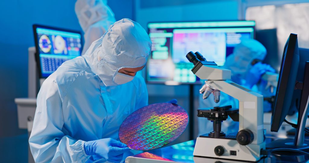
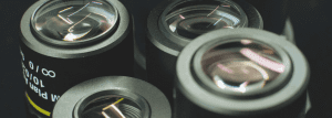
Custom optical objectives are crucial for semiconductor manufacturing and inspection, enabling the precision needed for advanced technologies. High numerical aperture (NA) objectives are particularly important for achieving the resolution required for sub-5nm feature sizes. The semiconductor industry relies heavily on a complex and interconnected supply chain to deliver the cutting-edge products and systems that power modern devices. Within this ecosystem, specialized companies that focus on the design and manufacture of high-precision optical components play a crucial role.
Key Applications
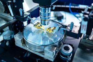
- Photolithography: High NA objectives focus UV or EUV light onto wafers with nanometer precision, creating intricate circuit patterns. They require high transmission at specific wavelengths (e.g., 193nm or 13.5nm), exceptional thermal stability, and minimized aberrations.
- Metrology and Inspection: Custom objectives can enhance tools like CD-SEMs, optical profilometers, and defect inspection systems. High NA lenses improve resolution and depth of field for precise dimensional measurements and sub-nanometer defect detection.
- Laser-Based Processes: Custom-built objectives ensure accurate beam focus and uniform energy distribution. They also mitigate thermal damage in applications like laser annealing, drilling, and patterning.
Challenges in Design
Designing a custom objective for specific applications is a complex process. Thermal stability is often of paramount importance due to the heat generated by high-power light sources. Precision manufacturing is essential, as even minor imperfections can degrade performance. Material selection is critical for optimal transparency and minimal birefringence at specific wavelengths. Cost and time constraints may also pose significant hurdles.Advantages of Custom Objectives:
Given numerous design and manufacturing challenges, why choose custom objectives? A custom-designed and manufactured objective can provide significant performance improvements, and you’re likely to see a number of advantages as you incorporate these objectives into your system:- High Precision and Accuracy: Sub-nanometer accuracy is achievable, enabling features down to 5nm and below to be patterned or inspected. Aberration correction can be optimized.
- Improved Yield and Defect Detection: Early defect detection and precise overlay control lead to high yields in advanced semiconductor nodes.
- Enhanced Resolution: High NA lenses enable smaller feature sizes for EUV lithography and nanometer-scale defect detection.
- Thermal Stability and Environmental Control: Low-expansion materials and controlled environments ensure consistent performance across a wide range of temperatures and environmental conditions.
- Flexibility and Tailored Solutions: Custom designs, including unique substrates, geometries, and manufacturing processes, meet the needs of specific applications.
- Supporting Advanced Technologies: Integration of meta-lenses and AI-assisted design further improves performance.
Limitations of Custom Objectives:
Although custom objectives are invaluable for many semiconductor manufacturing and inspection applications, they do have their downsides. Limitations of custom objectives include:
- High Costs: Design, prototyping, and testing are expensive and time-consuming.
- Manufacturing Complexity: Precise alignment during assembly is challenging.
- Long Development Time: Extended design and manufacturing time impact time-to-market.
- Limited Scalability: Custom optics often have a high per-unit cost due to low production volumes.
- Maintenance: Specialized maintenance and servicing are typically required for made-to-order optics.
- Material Limitations: Finding suitable materials for high-NA objectives under extreme conditions can be challenging.
- Contamination Sensitivity: EUV systems are highly sensitive to contamination.
High NA Systems in Semiconductor Applications
High NA objectives are essential for:- EUV Lithography: Achieving sub-5nm feature sizes for advanced nodes.
- Defect Detection: Detecting critical sub-nanometer defects.
- Metrology Tools: Analyzing surface and subsurface features.
- Meta-Lens Integration: Ultra-thin, high performance systems.
- AI-Assisted Design: Accelerating development through optimized design parameters.
- Sustainability: Energy efficiency and environmentally friendly materials.
- Advanced Node Technology: Enabling next-generation nodes.
- Photonics for Semiconductors: Driving efficiencies in various processes.
Avantier’s High NA Solutions for Semiconductor Applications
Custom objectives, particularly high NA systems, are indispensable for semiconductor manufacturing and inspection. Cutting edge optical research promises further advancements, enabling the optics industry to fully meet the evolving demands for semiconductor technology. Avantier’s products and services are specifically tailored to meet the exacting demands of this dynamic industry, providing the critical optical solutions needed for leading-edge semiconductor manufacturing and inspection equipment. We offer high NA microscope objectives and customized solutions with state-of-the-art technologies. Contact us today to discuss your next projects and find out more about how we can partner with you.


GREAT ARTICLE!
Share this article to gain insights from your connections!