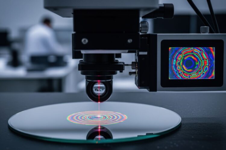
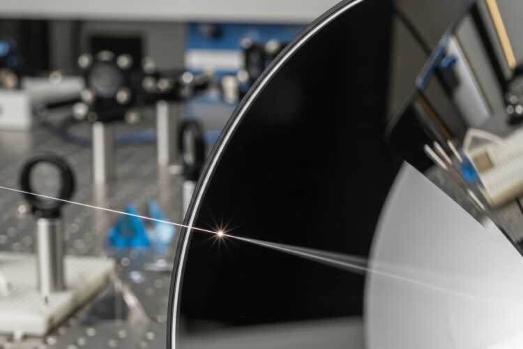
NIR Microscopy: Applications and Design Challenges in the 780–2500nm Range

Near-infrared (NIR) microscopy objectives (780–2500nm) are essential for “seeing through” opaque barriers.
By balancing high resolution with superior penetration, they enable deep-tissue biological imaging, subsurface semiconductor defect detection, and non-destructive material analysis.
Despite design challenges like specialized material selection (ZnS/Germanium) and complex aberration correction, modern NIR optics provide high-transmittance solutions (≥ 85%) that surpass the physical limits of visible light, driving innovation in both high-tech manufacturing and life sciences.

Read more
Precision Fabrication and Integration of Off-Axis Parabolic Mirrors

The Infinite Conjugate Microscope Objective—often referred to in industry as the infinity-corrected objective—has emerged as the cornerstone of advanced scientific instrumentation, precision inspection systems, and high-end manufacturing. It remains the optimal solution for unlocking new frontiers in microscopy and photonics.

Read more
High NA, Vacuum-Compatible Objective Lenses for Quantum Computing

Key Takeaways Objective lenses are essential in quantum computing for precise beam focusing, efficient fluorescence collection, and high-resolution qubit imaging. High numerical aperture boosts addressability and readout fidelity, while optimized working distance enables operation through vacuum or cryogenic interfaces. Wavelength-specific coatings, aberration correction, and window compensation preserve signal integrity. Vacuum and cryogenic compatibility, along with […]

Read more
Durable Optical Materials: Selection Guide for Space & High-Temperature Lens Systems
Durable Optical Materials for Harsh Environments

Key Takeaways: The integrity of any optical system designed for space, defense, or high-energy applications hinges entirely on selecting the right durable optical materials. For engineers in telescope manufacturing and satellite payload design, the challenge is twofold: achieving dimensional stability using thermally stable substrates against extreme thermal cycling, and maintaining clarity via radiation-hardened coatings under […]

Read more
Understanding Semiconductor Lithography

Key Takeaways Lithography systems are vital for precise circuit patterning in semiconductor manufacturing. Exposure methods like contact/proximity and projection are utilized to produce desired patterns.  Accurate alignment via global/local marks and interferometry is crucial, and  the light sources used dictate resolution.  Extreme Ultraviolet Light (EUV) enables production of the finest features. Innovations in lithography are […]

Read more