
Silicon photonics is the technology of photonic circuits on silicon substrates; The promise of high bandwidth, energy efficiency, and CMOS compatibility make silicon photonics central to next-generation computing.

The Quantum photonics tag focuses on photonic hardware developed specifically for quantum communication, sensing, and computation. Articles under this tag may highlight integrated photonic chips, waveguides, and coupling optics that route and process quantum states of light, as well as bulk optical components that interface chips with free-space or fiber systems. Topics can include loss minimization, phase stability, single-photon detection, and compatibility with telecom or visible wavelengths used in different quantum platforms. The tag emphasizes how design and material choices directly impact the fidelity and scalability of quantum photonic systems. For those working on quantum networks, sensors, or processors, these resources show how carefully tailored optics form the backbone of practical quantum photonic architectures. They also reflect Avantier’s understanding of the demands placed on components in cutting-edge quantum applications.
Silicon photonics is the technology of photonic circuits on silicon substrates; The promise of high bandwidth, energy efficiency, and CMOS compatibility make silicon photonics central to next-generation computing.
Quantum computing is one of humanity’s most ambitious technological frontiers, depending not only on quantum logic, but also on the tools that let us see and control the quantum world. Optical technologies and instruments remain critical to transforming quantum theory into practical, scalable reality.

Optical waveguides guide light using refractive index contrast, essential for quantum photonics circuits; They are the foundation of integrated quantum photonics. Achieving ultra-low loss, phase stability, high integration density, and thermal robustness is critical for scalable quantum architectures.
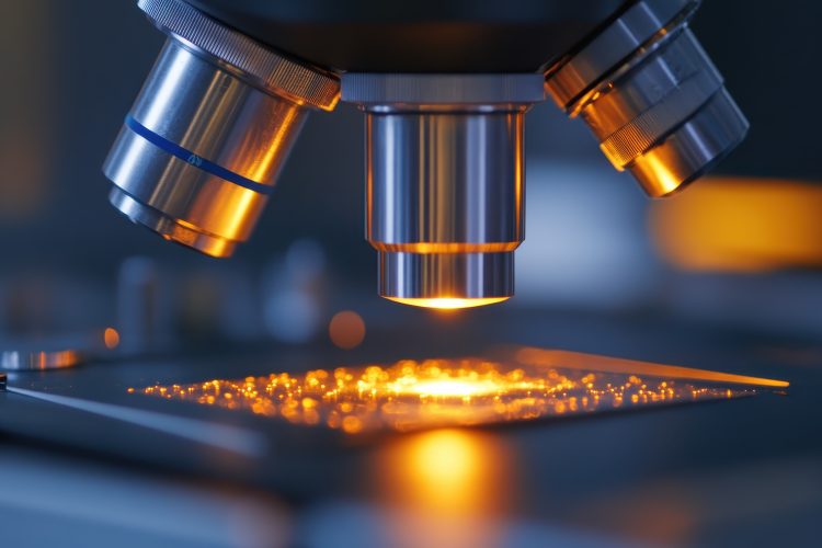
Lithography systems are essential to semiconductor manufacturing, enabling high-precision patterning through advanced exposure, alignment mechanisms, and specialized light sources to achieve high-resolution imaging.
