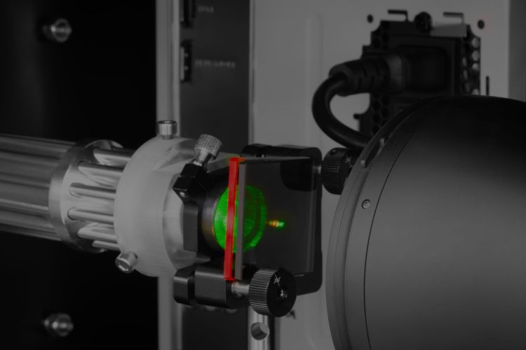
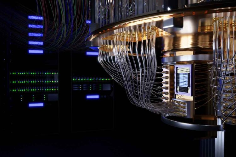
Space-based laser communications is a groundbreaking technology that enables better, faster, and more reliable data transmissions than traditional radio frequency technology.
Laser optics for surgery enable medical professionals to perform ultra-precise, minimally invasive surgical procedures.
Key Takeaways Lithography is crucial for precise, versatile, and efficient microlens array fabrication. It enables complex designs for advanced applications like laser beam shaping. Techniques like gray scale and direct laser writing lithography (DLWL) enhance efficiency and customization. Avantier leverages this technology for high-quality, tailored microlens array production. Lithography is a key technique in microlens […]
The reflector telescope is unique among telescopes because of its reflective design. Instead of using lenses to refract or bend light to form images, it uses a combination of curved surfaces and flat mirrors to reflect light for imaging.
The Advancements of ultrawide-field OCT in Retinal Imaging and Disease Management Avantier interviewed Dr. Jian, an expert in the field of ultrawide-field optical coherence tomography (OCT). We would like to extend our gratitude to Dr. Jian for his contribution to this discussion. Can you tell us about your path and how you started working on […]
With over two decades of experience in optical engineering and manufacturing, our company specializes in the design and production of high-precision microscope objectives.
A LiDAR sensor for robotics is more than simply another mechanical imaging system. LiDAR, short for Light Detection and Ranging, uses light in much the same way radar uses radio waves— to create a highly accurate, highly reliable map of surrounding objects.
Optical tweezer technology is a tool that utilizes highly focused laser beams to capture and manipulate tiny particles, such as cells and nanoparticles.
In today’s rapidly advancing technological landscape, semiconductor manufacturing pushes the boundaries of precision and miniaturization.
Custom optical objectives are crucial for semiconductor manufacturing and inspection, enabling the precision needed for advanced technologies.