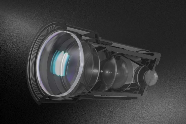
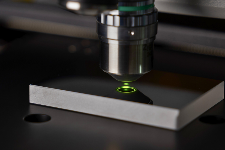
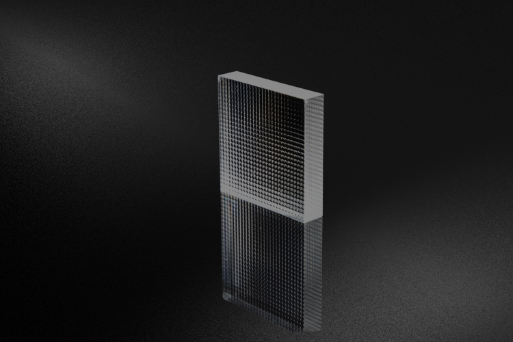
Understanding Diffractive Aspheric Lens

Key Takeaways Compact Design and High Performance: Diffractive aspherical lenses combine the benefits of aspheric and diffractive optics to deliver exceptional performance in a compact form factor, making them ideal for modern optical systems in industries like medical imaging, consumer electronics, and aerospace. Cost-Effective Solutions: By reducing the need for multiple components, diffractive aspherical lenses help lower manufacturing costs, streamlining production without sacrificing performance. Enhanced Optical Performance: These lenses excel in correcting both spherical and chromatic aberrations, providing superior image quality across a wide range of applications. Versatile Applications: The wide-ranging benefits of diffractive aspherical lenses enable their use in numerous cutting-edge industries, offering solutions for everything from portable devices to high-precision optical instruments. Manufacturing Highlights: Standard polishing methods don’t work on nonspherical lenses, but we have a number of special techniques at our disposal. Precision fabrication and alignment are crucial for achieving optimal performance, and ongoing advancements in production technologies are helping overcome key challenges. As optical systems continue to evolve, diffractive aspherical lenses are emerging as a transformative technology, especially in demanding IR applications. Combining the best attributes of aspheric and diffractive optics, these lenses offer high precision while reducing system size, making them ideal for industries where compactness and performance are crucial. With applications ranging from medical imaging to military reconnaissance and augmented reality (AR), diffractive aspherical lenses are revolutionizing the way we approach optical design. A diffractive aspheric lens is a powerful hybrid lens which offers multiple imaging benefits What Is a Diffractive Aspheric Lens? A diffractive aspheric lens incorporates both diffractive optical elements (DOEs) and an aspheric design. The diffractive optical elements are typically microstructure patterns in the substrate; they modify the phase of the light using diffraction effects, slowing it in some areas versus others.  This type of element is sometimes called a Fresnel zone plate.  Diffractive aspheric lenses are powerful optics designed to near absolute angular accuracy, with precise spherical and chromatic corrections built into the finished optic. What Makes Diffractive Aspherical Lenses Unique Traditional lenses often lack the precision necessary for modern infrared technologies, and attempts to reduce aberrations result in complex, bulky multi-element assemblies. Optical losses are another significant problem, as light is lost through dispersion. A diffractive aspherical lens is unique in the way it eliminates blur and increases resolution through an aspherical profile, even while it provides  precision light control  at a microscopic level through the DOEs. It minimizes light loss, and a single lightweight lens can be used to play the part of a large multi-element assembly. High quality aspheric diffractive lenses can be fabricated with up to 99.57% diffraction efficiency. Advantages of these lenses include: Aberration Correction Diffractive aspherical lenses excel at correcting both spherical and chromatic aberrations. This capability ensures sharper, clearer images, making them ideal for high-resolution applications. The integration of diffractive microstructures helps control light dispersion, resulting in more accurate focusing across a wide wavelength spectrum. Miniaturization and System Simplification One of the most significant advantages of diffractive aspherical lenses is their ability to reduce system size and complexity. By replacing multiple optical elements with a single hybrid lens, these lenses make it possible to design more compact systems without sacrificing performance. This is especially valuable in applications like endoscopes, where space is limited, and in portable devices such as wearables and drones. Cost Efficiency Incorporating diffractive microstructures into aspherical lenses reduces the need for multiple components, cutting down on both material costs and manufacturing time. This makes diffractive aspherical lenses a cost-effective solution for high-performance optical systems, particularly in consumer electronics and other price-sensitive markets. Enhanced Light Transmission Diffractive Optical Elements (DOEs) enhance the transmission of specific wavelengths of light, ensuring higher efficiency and reduced optical distortion. This results in more accurate color reproduction and improved imaging, both in the visible and infrared spectra. Manufacturing Diffractive Aspherical Lenses Lithography, replication molding, embossing, direct machining and diamond turning are all methods used to produce diffractive optical elements, but diffractive aspherical lenses for use with visible or IR light are most often produced with single point diamond turning (SPDT). For IR optics, germanium, zinc selenide, zinc sulphide, and silicon are substrates of choice. The most appropriate optical material will depend on both intended wavelength and the environment the optic will be used in.  A diffractive aspherical lens to be used at a 3–8 μm wavelength (MWIR), for instance, might use germanium as a substrate. Single crystal germanium has a high refractive index, good thermal sensitivity, and also has high permeability. Although it is difficult to machine because of its brittle nature, diamond turning can be used to create, grind and polish an aspheric diffractive lens with less than 5 nm surface roughness and a profile error of less than 0.3 μm. Small or half radius tools are then used to generate the sharp edge steps of the DOE. Spindle speed, feed rate, depth of cut and tool overhang are all parameters that must be carefully optimized in order to produce precision diffractive aspherical lenses.  Magnetorheological finishing (MRF) is a highly precise, computer-controlled finishing process that may then be used to ensure the highest quality diffractive aspheres.  Sophisticated techniques like MRF finishing enable us to make the most precise diffractive aspheric lenses Manufacturing Challenges The process of designing and fabricating a diffractive aspherical lens is complex and requires highly sophisticated techniques. Other special challenges we face when manufacturing these powerful lenses include: High Alignment Sensitivity and Low Tolerances Diffractive aspherical lenses are highly sensitive to microstructure alignment. Even minor misalignments during assembly can degrade optical performance. This makes precise assembly techniques, such as high-precision mounting and advanced metrology tools like interferometry and optical profilometry, essential for ensuring optimal lens performance. Wavelength Dependence While diffractive aspherical lenses offer high performance over a broad range of wavelengths, they are optimized for specific ranges. This limits their versatility in applications requiring multi-spectral imaging, and specialized lens designs may be needed. Surface Durability The microstructures on diffractive lenses are delicate and prone to damage, particularly in harsh environments. While protective coatings

Read more
Space-Based LIDAR and Hyperspectral Imaging

Key Takeaways for Space-Based LIDAR and Hyperspectral Imaging Technological Advancements: LIDAR offers precise 3D elevation data, while hyperspectral imaging captures detailed spectral bands for material analysis.  Complementary Insights: The integration of LIDAR’s structural data with hyperspectral imaging’s material identification provides a deeper understanding of environmental and geological processes.  Commercial Applications: These technologies are increasingly applied in agriculture, mining, forestry, water management, and urban development.  Future Innovations: AI, machine learning, and quantum sensing are revolutionizing the analysis and interpretation of remote sensing data. Challenges and Solutions: Advances in engineering are addressing issues related to sensor limitations, data processing, and environmental resilience in space Introduction  Space-based LIDAR (Light Detection and Ranging) and hyperspectral imaging are revolutionizing Earth observation. These advanced technologies allow scientists and engineers to measure topography, vegetation structure, water quality, and mineral composition with unprecedented accuracy. When used together, they can provide a multidimensional view of Earth’s surface, structure, and materials. These technologies play a critical role in tackling global challenges such as climate change, disaster response, and sustainable resource management.  Space-based LIDAR What Is Space-Based LIDAR?  Space-based LIDAR systems emit laser pulses from satellites to measure the distance to Earth’s surface. The time delay of the returning signal provides precise elevation data. Missions like NASA’s GEDI (Global Ecosystem Dynamics Investigation) and ICESat-2 use this technology to map 3D structures of forests, ice sheets, and terrain.  Applications of Space-Based LIDAR  Space-based LIDAR has many widely varying applications. A few highlights include: Forestry and Biomass Estimation: Measures canopy height and vertical structure to support accurate carbon stock assessments and REDD+ programs.  Topographic Mapping: Produces high-resolution Digital Elevation Models (DEMs) over large, often inaccessible areas.  Ice Sheet Monitoring: Tracks elevation changes to assess melting rates and their impact on sea level rise.  Urban Planning: Supports infrastructure design, flood modeling, and structural analysis for smart cities and disaster preparedness. LIDAR supports smart city initiatives by providing high-resolution data for infrastructure optimization, traffic management, and disaster resilience planning.  While LIDAR excels at mapping structure, hyperspectral imaging delivers powerful insights into surface composition, making the two technologies highly complementary. What Is Hyperspectral Imaging?  Hyperspectral imaging involves collecting data across hundreds of narrow, contiguous spectral bands. Each pixel in an image contains a full spectral signature, allowing identification of materials based on their reflectance properties. Instruments like NASA’s Hyperion and ESA’s PRISMA deliver this data from orbit, unlocking insights into land, water, and atmospheric phenomena. Applications of Hyperspectral Imaging  Hyperspectral imaging can be used together with LIDAR or on its own. Some of its applications include: Agriculture: Assesses crop health, identifies nutrient deficiencies, and monitors diseases across fields. For instance, hyperspectral imaging has been used to monitor crop health during droughts in California, enabling targeted irrigation strategies.  Geology and Mining: Detects specific minerals and lithologies for exploration and environmental monitoring.  Water Quality Monitoring: Tracks sediment loads, algal blooms, and chemical pollutants in rivers, lakes, and oceans. Recent studies have leveraged hyperspectral imaging to track harmful algal blooms in Lake Erie.  Disaster Response: Maps damage by identifying burned vegetation, flooded zones, and hazardous contamination after natural disasters.  Synergy Between LIDAR and Hyperspectral Imaging  The fusion of LIDAR’s structural data and hyperspectral imaging’s compositional insights enables a more complete understanding of ecosystems and geophysical processes. What does that mean, in practice? Here are three examples of synergistic applications. Wildfire Monitoring: Hyperspectral data detects burn severity and plant regrowth even while LIDAR quantifies changes in forest structure and fuel loads. For instance, the 2023 California wildfires were studied using fused LIDAR and hyperspectral data to assess burn severity and guide reforestation efforts.  Flood Detection and Management: LIDAR maps floodplain elevation and water extent while hyperspectral imaging evaluates water quality and contamination.  Habitat and Biodiversity Mapping: LIDAR reveals canopy gaps and terrain variation while hyperspectral data identifies plant stress and species diversity.  Together, these tools support precision conservation, sustainable resource use, and environmental risk mitigation. Manufacturing Challenges and Solutions The development and deployment of space-based LIDAR and hyperspectral imaging systems face several key challenges.:  Miniaturization & Weight Reduction: Space missions require compact, lightweight sensors. Solution: Advanced materials like carbon fiber composites and 3D printing help reduce weight without compromising structural integrity.  Optical Precision & Calibration: Ensuring high accuracy in sensors demands precise alignment and calibration. Solution: AI-driven calibration and automated alignment improve precision and reduce manual errors.  Radiation Hardening: Space sensors must withstand high radiation levels. Solution: Radiation-resistant coatings and GaN semiconductor materials enhance durability.  Power Consumption & Thermal Management: Efficient power use and heat dissipation are critical for long-term operation in space. Solution: Low-power electronics and passive cooling systems improve efficiency.  Data Processing & Transmission: Hyperspectral imaging generates massive datasets that need quick processing and transmission. Solution: AI-driven data compression and onboard edge computing optimize bandwidth use and processing speed.  Limitations of Space-Based Data Aside from the challenges above,  space-based LIDAR and hyperspectral imaging face several limitations:  Atmospheric Interference: Atmospheric composition can distort measurements, requiring complex correction algorithms.  Spatial and Temporal Constraints: Predefined satellite orbits result in gaps in data coverage and limited temporal resolution.  High Cost and Technical Complexity: Developing and launching space-based sensors remains expensive, limiting access to well-funded organizations.  Data Overload and Processing Challenges: Large datasets from hyperspectral imaging require significant computational power for real-time processing.  Limited Sensor Lifespan: Harsh space conditions can degrade sensors over time, though emerging self-healing materials may extend their durability.  Designing a space-based LIDAR/hyperspectral imaging system means working to overcome special challenges while being aware of inherent limitations. This powerful technology is becoming more accessible year by year, and many of these limitations may decrease in time.  Future Prospects  The next generation of space-based remote sensing will rely heavily on smarter, more automated platforms. We expect to continue to see advances in:  AI & Machine Learning: Enables rapid feature extraction, anomaly detection, and predictive modeling.  Quantum Sensing: Offers unprecedented sensitivity for detecting small changes in gravity, light, or magnetic fields. Quantum sensing can detect gravitational anomalies with unprecedented sensitivity, paving the way for advanced geological surveys from space.  Smaller Satellites

Read more
Space-based Laser Communications
Space-based laser communication systems like TBIRD have achieved fast space to earth data transmission.

Space-based laser communications is a groundbreaking technology that enables better, faster, and more reliable data transmissions than traditional radio frequency technology.

Read more
Importance of Lithography in Microlens Array Fabrication

Key Takeaways Lithography is crucial for precise, versatile, and efficient microlens array fabrication.  It enables complex designs for advanced applications like laser beam shaping.  Techniques like gray scale and direct laser writing lithography (DLWL) enhance efficiency and customization.  Avantier leverages this technology for high-quality, tailored microlens array production. Lithography is a key technique in microlens array fabrication, and the secret behind the precision manufacturing of many of the world’s highest quality and most innovative microlens arrays. Here we’ll look at just why it is so crucial for microlens array production, and a few of the ways these powerful methods can be used in practice at a world-class optical manufacturing company like Avantier. Microlens arrays have an important place in the modern world, and lithography is one of their most promising fabrication techniques. Why Lithography Even the simplest microlens arrays have specific and stringent manufacturing requirements, such as high uniformity over a large area. For some applications, the requirements are more complex, especially if they must be manufactured on a flexible or curved surface.  Lithography is important in microlens array fabrication because it offers: Precision, allowing the consistent, accurate manufacture of well-defined multi-level structures. For instance, lithography is well suited to producing  2 x 2 square centimeter arrays with feature sizes as small as 2 µm. Versatility. A variety of lithography techniques can be used to produce microlens arrays with different symmetries, structures, and sizes. Many lithography methods are also easily customizable, enabling factories like ours to produce arrays that meet our customers’ exact specifications. Efficiency. Lithography is an intrinsically efficient process, and there are some particular methods like DLWL which can be used to pattern large areas quickly for high fabrication speeds. Cost effectiveness. While cost ratios vary depending on the particular lithographic technique used, some techniques such as using transparency films as grey scale masks can decrease manufacturing times and complexity and reduce production costs. Suitability for Advanced Applications. Laser beam shaping and wavefront sensing require complex microlens array designs, and these are made possible with modern lithography techniques.  It is important to realize that lithography is not a one-route manufacturing process; a wide variety of techniques and materials are available that enable optical designers to optimize both the manufacturing process and the resulting arrays. An early stage in the MLA design process involves detailed modeling of expected interactions between a particular type of photoresist and propagated light, and different materials for both photoresist and substrate can be selected depending on desired final results.  Here we’ll look at two special techniques that can be used to manufacture microlens arrays with non-spherical geometries.  A Closer Look: Gray Scale Lithography Manufacturing a non-spherical microlens array using lithography is typically a multi-step iterative process using binary masks and reactive ion etching to produce multi-level structures in photo resist.  Using traditional methods, n repetitions of photolithography and careful attention to alignment are required to generate the n-level structures that are designed to serve as analogs of continuous 3D structures. An alternative method that can, in some cases, drastically increase manufacturing efficiency is grey scale lithography. In the place of binary masks, grey scale lithography utilizes grey scale photomasks (halftone chrome masks or high-energy beam sensitive glass masks are two options) to control light intensity. This enables the generation of 3D structures in just one exposure. The masks themselves transfer patterns onto the photoresist without size reduction and thus must be prepared at the appropriate micrometer scale; they can, however, be produced from large-scale  transparency films using microlens arrays to reduce the size. A Closer Look: Direct Laser Writing Lithography Another modern lithography technique that shows promise for manufacturing aspheric microlens arrays is DLWL, direct laser writing lithography. This enables flexible design, a customizable filling factoring arbitrary off axis operation for each microlens, and reduces manufacturing complexity significantly. At the same time, it is well suited for large scale manufacturing at high precision levels. A 2022 study using 12-bit direct laser writing lithography reported high fabrication speed, perfect lens shape control, and average surface roughness of less than 6 nm.  Lithography for Microlens Array Manufacturing at Avantier Avantier is at the forefront of microlens array manufacturing, and our state of the art equipment and lithography expertise enable us to produce high quality precision microns arrays to our customer’s requirements. Our expert designers can provide you with detailed modeling of light propagation and photoresist interactions, and help you choose the appropriate materials based on your desired outcomes.   Contact us today if you’d like more details on our manufacturing capabilities, to schedule a consult, or to place a custom order.  References Shiyi Luan, Fei Peng, Guoxing Zheng, Chengqun Gui, Yi Song, Sheng Liu. High-speed, large-area and high-precision fabrication of aspheric micro-lens array based on 12-bit direct laser writing lithography[J]. Light: Advanced Manufacturing 3, 47(2022)  Wu, H., Odom, T., and Whitesides,G. Reduction Photolithography Using Microlens Arrays: Applications in Gray Scale Photolithography. Analytical Chemistry, Vol. 74, No. 14, July 15, 2002 3269.  Yao, J. and Uttamchandani, D.G. and Zhang, Y. and Guo, Y. and Cui, Z. (2002) One-step lithography for fabrication of a hybrid microlens array using a coding grey-level mask. In: Conference on MEMS/MOEMS – Advances in Photonic Communications, Sensing, Metrology, Packaging and Assembly, 2002-10-28 – 2002-10-29.  Yuan, W., Li, LH., Lee, WB. et al. Fabrication of Microlens Array and Its Application: A Review. Chin. J. Mech. Eng. 31, 16 (2018).  Related Content

Read more
Reflector telescope

The reflector telescope is unique among telescopes because of its reflective design. Instead of using lenses to refract or bend light to form images, it uses a combination of curved surfaces and flat mirrors to reflect light for imaging.

Read more
Ultrawide-field OCT in Retinal Imaging and Disease Management

The Advancements of ultrawide-field OCT in Retinal Imaging and Disease Management Avantier interviewed Dr. Jian, an expert in the field of ultrawide-field optical coherence tomography (OCT). We would like to extend our gratitude to Dr. Jian for his contribution to this discussion. Can you tell us about your path and how you started working on optical coherence tomography (OCT)? I completed my undergraduate degree in optics in Shanghai, China, and then moved to Vancouver, Canada, to pursue my PhD in biophotonics. It was while I was studying there that I learned about OCT and its applications in eye imaging and adaptive optics. Under the guidance of my supervisor, a pioneering researcher in OCT, I had the opportunity to work with various OCT and imaging systems designed for both the anterior and posterior segments of the eye. A few years after earning my PhD in 2014, I was recruited by Dr. David Huang —one of the co-inventors of OCT— to join the faculty at Oregon Health & Science University (OHSU). There, I took part in developing OCT and other eye imaging systems. What challenges did you face in your research? Developing ultra-widefield OCT presents several challenges. The first challenge is the scan duration. The longer the procedure takes, the more uncomfortable a patient becomes. To minimize patient discomfort, a high-speed OCT system that utilizes advanced laser technology is needed. The second challenge involves imaging depth. We adopted a method to process data in real-time using a GPU, which allows us to accurately image the curved structure of the eyeball. The third and most significant challenge was related to optics. We needed components that could provide high-quality, high-resolution imaging, but the existing designs did not meet our specifications. We also experimented with ophthalmic lenses from other imaging modalities, but they lacked the optical quality and performance necessary for our research objectives. Retinal Imaging by OCT (Copyright: Dr. Yifan Jian, OHSU University) How do you collaborate with Avantier? After conducting various studies, we determined that existing ophthalmic lenses were unsuitable for ultra-widefield OCT. There was just one solution: we had to design and manufacture our own custom optics. This process required us to gain a deeper understanding of optical design and optical software in order to develop a high-performance lens system. It was at this time that we discovered Avantier could produce cost-effective and high-quality optical components. Their approach was more streamlined and affordable than the approaches of other companies, which was particularly important for us as we were new to custom lens design. Today our ultrawide field OCT systems are capable of delivering impressive results. They provide high-quality ultra-widefield images that are utilized in clinics for conditions such as diabetic retinopathy and in neonatal intensive care units to screen premature infants for retinopathy of prematurity. Our collaboration with Avantier has broadened the possibilities of ultra-widefield OCT, and the custom optics we incorporated enable our systems to attain high levels of performance in both research and clinical settings. A sample picture of the eyepiece Research on past and future developments in OCT Our ultra-widefield OCT systems have significantly expanded the capabilities of retinal imaging. Handheld and desktop configurations facilitate comprehensive analysis of both the anterior and posterior segments of the eye, with crucial applications for conditions like diabetic retinopathy and age-related macular degeneration. One of the most significant advancements in my lab has been the development of a system that can capture an almost perfect 3D reconstruction of the entire eye in a single scan. This technology is particularly beneficial for managing myopia, allowing us to track changes in the shape of the eye. We also employ ultra-widefield OCT in ophthalmic oncology to accurately measure tumors within the eye. OCT offers extremely detailed structural information and higher resolution than traditional imaging methods like MRI and ultrasound. Increasing imaging speed has been another major focus of our work. We have developed a new system that projects an entire line of light rather than scanning a single point. This innovation allows for parallel image acquisition, significantly improving processing speed. We are also exploring ways to enhance tissue contrast to reveal retinal layers that were previously difficult to differentiate. I believe that speed will be a defining factor for the future of OCT. Commercially available systems are still relatively slow compared to research-grade devices. Faster OCT will facilitate imaging of a larger field of view and enable functional assessments, such as opto-retinal photography, which allows for real-time evaluation of photoreceptor function. In our research, we will continue to explore mechanisms for achieving higher resolution and better contrast, including oxygen saturation mapping. Thoughtful optical design will be critical in pushing the boundaries of what OCT can uncover. One more aspect I would like to highlight is my research on adaptive optics for high-resolution imaging. We have developed a system that iteratively optimizes image quality without the need for a wavefront sensor. This technology has been successfully applied to imaging small animals. My research on retinopathy of prematurity is another area in which we’ve been able to make a meaningful difference. Utilizing ultra-widefield handheld OCT, we have redefined diagnostic criteria for this condition and identified new biomarkers that traditional imaging could not detect. These new criteria show great promise for early diagnosis and treatment. About Dr. Yifan Jian  Dr. Yifan Jian is an Associate Professor at Casey Eye Institute specializing in optical imaging. He earned his Ph.D. from Simon Fraser University in 2014 and later joined Oregon Health and Science University (OHSU) to advance OCT technology for ophthalmic imaging, including real-time processing and adaptive optics innovations. Currently, his main research focus is advancing ultrawide-field OCT systems. From Avantier It is an honor to support Dr. Jian’s research as an optical solutions provider. His work has a great impact on the world, advancing science and biomedical technology and providing real value, especially for premature infants and their families. As an optical manufacturer and as a member of society, we are grateful to dedicated individuals like Dr. Jian who

Read more