
Key Takeaways
- Lithography is crucial for precise, versatile, and efficient microlens array fabrication.
- It enables complex designs for advanced applications like laser beam shaping.
- Techniques like gray scale and direct laser writing lithography (DLWL) enhance efficiency and customization.
- Avantier leverages this technology for high-quality, tailored microlens array production.
Lithography is a key technique in microlens array fabrication, and the secret behind the precision manufacturing of many of the world’s highest quality and most innovative microlens arrays. Here we’ll look at just why it is so crucial for microlens array production, and a few of the ways these powerful methods can be used in practice at a world-class optical manufacturing company like Avantier.
Why Lithography
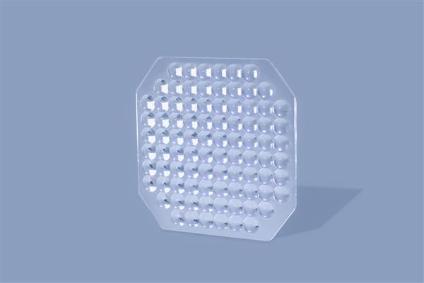
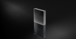
Even the simplest microlens arrays have specific and stringent manufacturing requirements, such as high uniformity over a large area. For some applications, the requirements are more complex, especially if they must be manufactured on a flexible or curved surface. Lithography is important in microlens array fabrication because it offers:
- Precision, allowing the consistent, accurate manufacture of well-defined multi-level structures. For instance, lithography is well suited to producing 2 x 2 square centimeter arrays with feature sizes as small as 2 µm.
- Versatility. A variety of lithography techniques can be used to produce microlens arrays with different symmetries, structures, and sizes. Many lithography methods are also easily customizable, enabling factories like ours to produce arrays that meet our customers’ exact specifications.
- Efficiency. Lithography is an intrinsically efficient process, and there are some particular methods like DLWL which can be used to pattern large areas quickly for high fabrication speeds.
- Cost effectiveness. While cost ratios vary depending on the particular lithographic technique used, some techniques such as using transparency films as grey scale masks can decrease manufacturing times and complexity and reduce production costs.
- Suitability for Advanced Applications. Laser beam shaping and wavefront sensing require complex microlens array designs, and these are made possible with modern lithography techniques.
It is important to realize that lithography is not a one-route manufacturing process; a wide variety of techniques and materials are available that enable optical designers to optimize both the manufacturing process and the resulting arrays. An early stage in the MLA design process involves detailed modeling of expected interactions between a particular type of photoresist and propagated light, and different materials for both photoresist and substrate can be selected depending on desired final results.
Here we’ll look at two special techniques that can be used to manufacture microlens arrays with non-spherical geometries.
A Closer Look: Gray Scale Lithography
Manufacturing a non-spherical microlens array using lithography is typically a multi-step iterative process using binary masks and reactive ion etching to produce multi-level structures in photo resist. Using traditional methods, n repetitions of photolithography and careful attention to alignment are required to generate the n-level structures that are designed to serve as analogs of continuous 3D structures.
An alternative method that can, in some cases, drastically increase manufacturing efficiency is grey scale lithography. In the place of binary masks, grey scale lithography utilizes grey scale photomasks (halftone chrome masks or high-energy beam sensitive glass masks are two options) to control light intensity. This enables the generation of 3D structures in just one exposure. The masks themselves transfer patterns onto the photoresist without size reduction and thus must be prepared at the appropriate micrometer scale; they can, however, be produced from large-scale transparency films using microlens arrays to reduce the size.
A Closer Look: Direct Laser Writing Lithography
Another modern lithography technique that shows promise for manufacturing aspheric microlens arrays is DLWL, direct laser writing lithography. This enables flexible design, a customizable filling factoring arbitrary off axis operation for each microlens, and reduces manufacturing complexity significantly. At the same time, it is well suited for large scale manufacturing at high precision levels. A 2022 study using 12-bit direct laser writing lithography reported high fabrication speed, perfect lens shape control, and average surface roughness of less than 6 nm.
Lithography for Microlens Array Manufacturing at Avantier
Avantier is at the forefront of microlens array manufacturing, and our state of the art equipment and lithography expertise enable us to produce high quality precision microns arrays to our customer’s requirements. Our expert designers can provide you with detailed modeling of light propagation and photoresist interactions, and help you choose the appropriate materials based on your desired outcomes. Contact us today if you’d like more details on our manufacturing capabilities, to schedule a consult, or to place a custom order.
References
- Shiyi Luan, Fei Peng, Guoxing Zheng, Chengqun Gui, Yi Song, Sheng Liu. High-speed, large-area and high-precision fabrication of aspheric micro-lens array based on 12-bit direct laser writing lithography[J]. Light: Advanced Manufacturing 3, 47(2022)
- Wu, H., Odom, T., and Whitesides,G. Reduction Photolithography Using Microlens Arrays: Applications in Gray Scale Photolithography. Analytical Chemistry, Vol. 74, No. 14, July 15, 2002 3269.
- Yao, J. and Uttamchandani, D.G. and Zhang, Y. and Guo, Y. and Cui, Z. (2002) One-step lithography for fabrication of a hybrid microlens array using a coding grey-level mask. In: Conference on MEMS/MOEMS – Advances in Photonic Communications, Sensing, Metrology, Packaging and Assembly, 2002-10-28 – 2002-10-29.
- Yuan, W., Li, LH., Lee, WB. et al. Fabrication of Microlens Array and Its Application: A Review. Chin. J. Mech. Eng. 31, 16 (2018).


GREAT ARTICLE!
Share this article to gain insights from your connections!
